138 KiB
| created_at | title | url | author | points | story_text | comment_text | num_comments | story_id | story_title | story_url | parent_id | created_at_i | _tags | objectID | year | |||
|---|---|---|---|---|---|---|---|---|---|---|---|---|---|---|---|---|---|---|
| 2015-06-03T16:44:28.000Z | Concise electronics for geeks (2010) | http://lcamtuf.coredump.cx/electronics/ | luu | 167 | 22 | 1433349868 |
|
9653898 | 2010 |
Concise electronics for geeks
Concise electronics for geeks
Copyright (C) 2010 by Michal Zalewski <lcamtuf@coredump.cx>
There are quite a few primers on electronics on the Internet; sadly, almost all of the top hits resort to gross oversimplifications (e.g., hydraulic analogies), or convenient omission, when covering subtle but incredibly important topics such as the real-world behavior of semiconductors. There are some exceptions - but they often suffer from another malady: regressions into mundane, academic rigor, complete with differential equations and complex number algebra in transient analysis - a trait that is highly unlikely to be accessible, or even useful, to hobbyists.
The goal of this guide is to bridge this gap; it should give you an anatomically correct insight into the underlying physical phenomena needed to accurately understand the behavior of semiconductors, capacitors, or inductors - but should be far more readable and way shorter than a typical academic textbook. The target audience is people who want to meaningfully tinker with more complex electronic circuits, or perhaps understand how computers really work - but for whom getting there is not meant to be a full-time job.
The physics of conduction [link]
As you probably recall from your school years, the dated but still useful Bohr model of the atom explains that atoms consist of a dense center (nucleus) with a variable number of protons and neutrons. This center is surrounded by a distant cloud of small, elementary particles called electrons occupying a number of discrete energy states around it.
The two most important forces governing the atomic structure are: the powerful but short-range residual strong force that binds the protons and neutrons together; and a significantly weaker but far-reaching electromagnetic force that causes subatomic particles carrying elementary charges to create electric fields, repelling similar charges, and attracting dissimilar ones. Charges traveling in relation to each other are also mutually subjected to magnetic fields.
Protons have an inherent, elementary positive charge; electrons have an identical charge with the opposite sign; and both produce a gradually vanishing (but infinite) electric field around them. This field is customarily visualized by observing how it would affect a positive charge in its vicinity: field lines are shown to be radially emanating away from positive charges, or toward negatives ones.
Neutrons don't generate and do not respond to electric fields - but are affected by magnetic fields created by charges in motion; this is an artifact of their quark makeup.
The positive electric charge (Q) of 6.24 * 1018 protons is known as one coulomb (C); you don't need to remember this number: its only significance is that it corresponds neatly to other SI units used to measure related physical phenomena.
The electromagnetic force causes protons to attract electrons, and forces the captive electrons to orbit the nucleus; it also causes protons to repel each other - but this effect is easily overcome by the strong nuclear force that holds the center of the atom together. Given the opportunity, any sufficiently stable atomic nucleus will generally seek to accumulate a number of electrons matching the number of protons, in order to form an electrically neutral particle.
The strongly bound and heavy nuclei of stable isotopes do not undergo any structural changes under everyday circumstances. The electrons occupying the energetic, outer (valence) orbitals of an atom are a very different story; they are usually attracted to the nucleus fairly weakly, and can engage in two rather interesting behaviors:
- Some valence electron configurations are energetically preferred over others, due to the complex proton-proton and electron-electron interactions and quantum probability distributions that affect the geometry of the nuclear electromagnetic field. Because of this, in favorable conditions, atoms may be willing to share some of their electrons with neighbors, forming electrically neutral molecules held together by the electromagnetic force - and bringing us chemistry as we know it.
Three primary types of intramolecular bonds are recognized, depending on the exact nature of this exchange: covalent, ionic, and metallic. This last category is of particular interest: shared valence electrons in metals are so weakly bound, that they enjoy largely unhindered mobility through the crystal lattice, and are seemingly not tied to any particular atom - forming what is called an electron gas distributed through the material.
- Certain atoms or molecules may be not particularly strongly opposed to acquiring some additional electrons, or losing some of their own, without firmly attaching to any other single molecule - gaining a net negative or positive electrical charge in the process. Such charged particles are known as ions (anions and cations, respectively).
Ion formation may be driven by certain chemical reactions, by the action of polar solvents on some substances, by certain types of energetic collisions - or even by simple mechanical action: when materials of different affinity to electrons are brought into contact and then pulled apart, a significant charge imbalance may form. It is worth noting that with sufficient energy, almost any substance will eventually form free ions; that said, materials in which ions are not formed easily under normal operating conditions are known as insulators.
In dissociated solutions or in plasma, ions themselves are fairly mobile, moving around in response to electric fields and other processes; electrochemistry studies these behaviors in great detail, with batteries being one of the most important applications of this principle. In solids, however, ions typically do not enjoy appreciable mobility. Therefore, many materials where ions can form with ease are still non-conductive: their surfaces may accept localized charges easily, but these charges do not move from one point to another on their own. Such materials may be useful for energy storage, but are poorly suited for signal distribution and processing.
As hinted earlier, metals are a special case in the world of solids, however: their crystal lattice may be considered to consist of (still immobile) metal cations, surrounded by mostly-free-roaming electrons. These electrons are not really bound to any specific atom; and if any localized charge imbalance is created by depositing or removing electrons, this imbalance gets equalized through the conductor at a significant fraction of the speed of light. It is important to note that the electrons themselves don't move through the medium nearly as fast - in fact, their traverse speed in a metallic conductor is usually measured in millimeters per second; think of pressure equalization in a fluid, instead. This effect in response to an externally applied, electromotive force (say, a chemical reaction that forcibly takes electrons from one place and shoves them elsewhere) is known as the flow of electricity.
In solid-state conductors, negatively-charged electrons are the only real, mobile charge carriers. Their positive counterpart - the positron - is a form of antimatter, and is not commonly encountered on Earth (although it can certainly be spotted at times).
The curious case of semiconductors [link]
In metals, there is an abundance of mobile electrons in the conduction energy band at any given time because there is no energetic band gap between the valence and conduction bands - i.e., valence electrons already have the range of energies needed to move around in the material at will. Conversely, in insulators, there are no virtually no mobile charge carriers, because the band gap is large enough not to be casually crossed by valence electrons under normal operating conditions.
Semiconductors are a special, intermediate case: similar to insulators, they have a band gap - but the gap is small enough to allow electrons to be periodically "knocked out" of their usual orbit and into the mobile conduction band, simply due to the inherent thermal vibration of atoms in the crystal lattice. In absence of an external electric field, these electrons quickly return to their original positions, and the process repeats over and over again.
When a sufficiently strong electric field is applied, the picture changes slightly: the temporarily liberated electrons will immediately dart off toward the more positive region (a direction said to go "against" the direction of the electric field) - leaving holes in the valence bands of their original hosts. Nearby electrons closer to the more negative region are also subject to the same electromotive force, and will be eager to jump into that energetically favorable hole, in leaving a new hole at their original location. Over time, this will seemingly cause holes to drift in the crystal lattice "along" the field. The process ends with the liberated electron arriving at one edge of the semiconductor, ready to continue its journey elsewhere should any opportunity present itself; and with the hole bubbling up toward the other end, willing to accept any externally donated electrons. This form of charge transfer permits conduction, albeit only to a very limited extent (only a limited number of excited charge carriers is available at any given time, and due to spontaneous recombination, their lifetime is short). Of course, poor conductivity is not a significant feat by itself - about the only interesting property of this material is that more electrons get knocked into the conduction band when the material is exposed to light (with photons impacting the surface and transferring their energy to it) - giving birth to photoresistors and related light-sensitive electronic devices.
The situation gets slightly more remarkable once the material is doped with certain other, closely related atoms. In n-type semiconductors, the dopant is a substance eager to donate its own weakly bound electrons to plug holes - before the temporarily excited electrons rightfully belonging to the doped material have a chance to return to their original state. This creates an abundance of long-lived negative charge carriers in the conduction band, in a stable material that has no net electrical charge (every dopant cation is offset by a free electron). These electrons will happily drift against any externally applied electric field with little effort.
In p-type semiconductors, on the other hand, the dopants are quick to snatch and trap any excited electrons with more force than the atoms from which the electrons originally came from. This achieves the opposite effect: an abundance of long-lived holes that want to accept any externally supplied wandering electrons into their valence bands. In an external field, this sea of holes will allow other electrons to surf from one atom to another without too much work (although jumping between holes requires a bit more energy than just drifting in the conduction band).
Because of the continuous availability of long-lived charge carriers, both of these materials are highly conductive - but by themselves, perhaps not particularly exciting. The really interesting bit is when a p-n junction is formed by bringing these two types of semiconductors into contact, however: initially, some of the idle electrons from the n-type material will enter the p-type semiconductor to recombine with nearby holes; and p-type semiconductor holes will seemingly "propagate" across the junction when some nearby, temporarily excited valence electrons from the n-type material are captured on the p-type side, leaving holes in their original locations. This leads to the formation of a thin depletion layer, with very few mobile charge carriers available (and therefore, with rather poor conductivity). The formation of this layer is a self-limiting effect, though: with no external supply of charges, the recombination leaves the dopant ions in the vicinity of the junction unpaired, and the resulting electrostatic field (positive on the n-type side, and negative on the p-type side) eventually becomes strong enough to capture and hold any wandering electrons and holes, and prevent them from getting across the junction.
Applying an external field to the junction in the direction identical to this intrinsic field - a process called reverse biasing - only serves to pull charge carriers further away, and therefore widen the depletion layer; appreciable conduction will not occur under these circumstances, at least until the field is strong enough to trigger avalanche breakdown or a similar phenomenon.
Forward biasing the junction, on the other hand, will push the remaining charge carriers on both sides toward the junction, overcoming the internal field. If an external supply of charges is maintained, this allows continuous and efficient hole-electron recombination in the junction area, and the flow of current: n-type semiconductor accepts electrons to offset unbalanced cation charges, and the p-type semiconductor gives them up and frees up holes to avoid developing an unbalanced negative charge of its own. As a bonus, recombination is sometimes accompanied by photon emission, as excited conduction band electrons finally drop to a lower energy level after finding a spot in nearby valence shells, and then continue the ride hole-jumping in the valence band.
This field-controlled, unidirectional conduction of semiconductor junctions is one of the more important discoveries in the history of electronics - allowing a large number of solid-state nonlinear or active components to be built; we will discuss them in more detail later on.
Core concepts in electrical circuits [link]
Current (I) [link]
Current is the measure of the flow of electric charges through a selected section of the circuit. The unit of current - ampere (A) - is one of the base SI units, defined as the flow of some 6.24 * 1018 elementary charges (1 coulomb) per second.
The flow of current is the mechanism by which electrical circuits can perform useful work. Naturally, unbalanced charges deposited in a variety of materials may generate electromagnetic fields even when no current is actively flowing, and these fields may in turn affect nearby objects, change the distribution of other charges in conductors, or control the behavior of semiconductor junctions; that said, depositing these charges in the first place requires the flow of current.
Current through a conductor is generally expressed as a non-negative, absolute value, no matter which way it is flowing. The direction of the flow - for historical reasons, marked in the direction opposite to the actual direction of electron travel, i.e. from a positive pole of the supply to the negative one - is usually conveyed when describing the voltage instead (see later on).
Rudimentary ammeters can be designed to measure currents by detecting the magnetic field generated by charges in motion, for example by placing a permanent magnet on a spring near a coiled conductor; ideal ammeters would not impede the flow of current in any way, although in practice, some power is always dissipated.
Resistance (R) [link]
Resistance is the measure of opposition to the steady flow of an electric current. With the exception of superconductors, all conductive materials impede the flow of electrons to some extent - generally through a linear, time-invariant effect comparable to aerodynamic drag; the energy wasted to overcome the drag excites the medium, and is eventually dissipated as heat.
The unit of resistance - ohm (Ω) - is a derived SI unit, defined as the resistance of a conductor that, when subjected to a steady current of one ampere, dissipates one watt (W) of heat - that's one joule (J) per every coulomb of charge moved around.
In any uniform metallic conductor, the resistance is roughly equal to its length, times material-specific resistivity constant, divided by the cross-section of said conductor; some temperature dependency is also present. In practical circuits, conductors are generally selected so that the effects of their resistance are negligible; a specialized class of components, known as resistors, is used to introduce predictable, linear resistance into the circuit, instead. Resistors with a very significant temperature dependency are known as thermistors, but are used rarely.
Some materials may impede the flow of currents in a time-dependent manner, usually associated with the creation of magnetic or electric fields; this effect is not considered to be resistance, and is studied separately. Other materials may exhibit resistance patterns that are time-invariant, but vary in relation to some other parameter (e.g., in semiconductor junctions that respond to the magnitude and direction of external electromotive forces); this effect is still resistance, but such devices are not called resistors.
Voltage (V) [link]
Voltage across any two points in the circuit has several definitions, but most intuitively, can be understood as the measure of an electromotive force that would drive a current through a hypothetical conductor connected across these two points.
This force does not depend merely on the difference in the number of accumulated elementary charges - but also on the "pressure" these charges are under to leave their current spots, due to the influence of resulting electric and magnetic fields. As a simple illustration, consider depositing 100 electrons on two conductive, reasonably distant plates - one of them large, and one small. Electrons deposited on the smaller plate will be packed more densely, and therefore, electric repulsion between them will be far more violent than in the other material. When the two elements are bridged with a conductive path, some current will briefly flow as charge densities (and not counts) equalize.
The unit of voltage - volt (V) - is a derived SI unit defined as the amount of electromotive force needed to induce the current of one ampere across a conductor with the resistance of one ohm.
In any electrical circuit, voltage measurements are meaningful only if relative to a clearly defined reference point; many direct current circuits use a common rail connected to the negative pole of a two-pole battery as a "ground", customarily defined as 0 volts - in which case, all measurements are implicitly understood to relate to this point. That said, the voltage between this rail and any other external, insulated object is essentially undefined: one man's 0V may be somebody else's -20,000V, even if simply due to electrostatic charge buildup. A well-designed physical connection to soil may provide a common 0V reference, but this comes with its own perils, and therefore, is used only when absolutely necessary.
In almost all signal-processing circuits, useful information is encoded using changing voltage levels, rather than current magnitudes; exceptions happen, but are fairly rare.
Specifying steady voltages is not rocket science. but some ambiguity exists when it comes to constantly changing voltages in alternating current circuits, where the direction of current flow periodically reverses. In these settings, three different values may be used:
-
Peak voltage (Vpeak): measures voltage amplitude of the waveform in reference to its center point. This approach is commonly employed when dealing with small-signal AC circuits.
-
Peak-to-peak voltage (Vp-p): measures voltage difference between the lowest and highest voltage observed in the waveform (equal to
2 * Vpeak). This is conceptually similar to how signal voltage is measured in DC circuits. -
Root mean square voltage (VRMS): uses the value of an equivalent DC voltage that would deliver the same power to the load (about
0.71 * Vpeakfor sine wave currents). This approach is particularly common in electrical power distribution calculations. This graph demonstrates the difference more succinctly:

Always be aware which measurement method is being used; for example, "110V" AC mains voltage is actually given as RMS; this means that the actual sine wave swing is 154V, and peak-to-peak voltage is close to 310V (ouch!).
Ohm's law [link]
Ohm's law is one of the most important rules describing the behavior of electrical circuits by formalizing the relationship between currents, voltages, and resistances - and a pretty straightforward one, too. The law states that the steady current flowing through a conductor is directly proportional to the voltage applied to it, and inversely proportional to its resistance:
I = V/R
The same equation tells us that the voltage measured across a conductor must be equal to the steady current applied to it, times resistance:
V = IR
And lastly, that the resistance of a conductor can be derived from the observed current and the voltage across its terminals:
R = V/I
This law is what makes resistors such useful components: they can be used to limit the current flowing through parts of the circuit to a specific, desired value; or, by creating voltage differences across resistor terminals, to create lower voltages for a variety of purposes.
Ohm's law also makes it easy to turn ammeters into voltmeters and ohmmeters. Voltmeters can simply measure the very low current flowing through when a large resistor of known value is placed across the test points (this resistor needs to be large enough not to disrupt the circuit in an appreciable way) - and then compute the voltage according to the V = IR rule; ohmmeters may be constructed by applying a known voltage to an unknown resistive load, measuring the resulting current, and then solving the equation for R.
Joule's law [link]
Power (P) is a measure of the rate at which work is performed, or at which energy is converted into another form. In electrical circuits, a form of Joule's law gives us the following formula:
P = IV
...where I is the current through a component, and V is the observed voltage drop. This relationship is actually intuitive: if there is no current flowing, obviously no useful work is being done by a circuit; and if no voltage drop occurs, all the current must be passed as-is, rather than utilized in any way.
Electrical energy may be dissipated as heat or radiation, converted to motion, stored in electromagnetic fields, in electrochemical reactions, and so forth; in all cases, the equation gives you an accurate picture of the sum of all the processes at work, based on the observed or predicted voltage and current alone.
Heat dissipation is of particular interest in electronics, as it must be kept in check to avoid destroying resistive loads. By combining Joule's law and Ohm's law, it can be shown that the heat dissipated by a resistor is given by any of these two equations:
P = I²R
P = V²/R
This is pretty useful: you can use these rules to show that it's impossible to exceed the power rating of a 1/4 watt, 150 Ω resistor working in a 5V circuit; and that a 15 Ω resistor will light up the night sky in that same setting, unless the current through it is limited by other means.
Intermission: working with decibels [link]
In component datasheets and some calculations, engineers often opt to express the ratio between power quantities in terms of a somewhat arbitrary but convenient logarithmic measure - decibels (dB):
LdB = 10 * log10(P1 / P2)
For example, a 25% increase in the power of an acoustic wave is equal to about +1.0 dB; a two-fold increase will be equal to about +3 dB; and a 100-fold increase will be +20 dB.
In electronics, it is usually more desirable to compare voltages and signal amplitudes, rather than to directly measure power. Since the relation between voltage and power is usually quadratic - in these uses, decibels are calculated using a slightly different formula:
LdB = 10 * log10(V1² / V2²) = 20 * log10(V1 / V2)
Therefore, a 50% increase in voltage is +1.0 dB, a two-fold increase is about +6 dB, and so forth. There is nothing profoundly significant about decibels, but they will crop up every now and then - so it's best to get this over with right away.
Time-dependent currents [link]
Some types of linear electronic components may exhibit time-dependent (and therefore, signal frequency dependent) current characteristics. This pattern is generally associated with the (reversible) storage of some of the supplied energy, most commonly in the form of electromagnetic fields.
Capacitance (C) [link]
When two conductive plates are brought close to each other, it becomes unusually easy to store opposing electrostatic charges on them: the strong electromagnetic field caused by electrons drawn away from one of the plates will be largely offset by a symmetrical field caused by charges pushed onto the other plate. The closer the plates are together, the larger surface area they have, and the better the medium between them is at guiding and amplifying the resulting electric field (due to the field-induced alignment of dipoles) - the greater number of elementary charges can be deposited on one end, and removed on the other, before the electromotive force opposing this process becomes as strong as the voltage driving it. Note that this works only if the charge transfer is symmetrical, though: if charge carriers are not efficiently removed from one of the plates, they can't be efficiently added on the other one, not without having to fight a much stronger, unbalanced electric field.
Capacitance is the measure of this phenomenon: the ratio of the number of charges deposited (in coloumbs), versus the electromotive force needed to deposit them (in volts):
C = Q/V
Another way to look at it is that one farad (F) - the unit of capacitance - corresponds to the steady current of one ampere being supplied for one second, and resulting in one volt potential difference forming across the plates:
C = I*t/V
Most electronic components are designed to keep their inherent capacitance at a negligible level; some parasitic capacitance may develop between parallel wires or circuit board traces, but this is a concern only in certain specialized applications. Intentional capacitances are usually introduced where needed with dedicated components - capacitors; these devices usually consist of two long ribbons of a metallic conductor, separated by dielectric film.
The interesting property of capacitors is that when subjected to a constant external voltage, they initially allow the flow of current - even though electrons do not actually pass through the gap, they can perform useful work in other parts of the circuit on their way onto, or away from, the plates. This current will gradually drop to zero as the voltage across the plates approaches the supply voltage, though - and eventually, all apparent conduction will cease:

When the capacitor is then disconnected from the charging source, it will retain the charge imbalance (in theory, indefinitely); the stored charges will create a transient current as soon as a conductive path is created across the capacitor terminals, a process that will return the stored energy, and return the capacitor to its discharged state. The speed at which this happens is given by a differential equation, but it's usually sufficient to know the following (R is resistance through which the device is charged or discharged):
t = 1/3RC → I = 75%, V = 25%
t = 1/2RC → I = 60%, V = 40%
t = 2/3RC → I = 52%, V = 48%
t = 1RC → I = 37%, V = 63%
t = 2RC → I = 14%, V = 86%
t = 3RC → I = 5%, V = 95% - practically fully charged
t = 4RC → I = 2%, V = 98%
t = 5RC → I = 0.7%, V = 99.3%
Capacitors often serve as a simple energy-storage device - but their other interesting property is that while they largely block conduction for low-frequency currents (spare for the brief time when they are getting charged), they allow apparent conduction at higher frequencies: if the current is reversed before the charging is complete, there is a continuous reciprocating motion of charges through the surrounding circuit. This effect is capacitance-, current-, frequency-, and waveform-dependent - but in essence, any given capacitor charged and discharged with a well-controlled alternating current acts as a simple high-pass filter; average current through one particular capacitor in function of the frequency of the driving sine wave is shown in this graph:

We will discuss frequency filters in more detail later on.
Inductance (L) [link]
As mentioned earlier, charged particles tend to interact with other particles moving in relation to them. On a macroscopic scale, this manifests itself as a magnetic force between materials with aligned electron spins; and more interestingly, as an electromotive force experienced by conductors subjected to magnetic field gradients in space or in time. In essence, any varying magnetic field, perhaps created by a varying current in a conductor or by moving a permanent magnet around, may induce transient voltage in any other conductor subjected to this influence; this process is the subject of Faraday's law of induction.
Inductors are a class of devices consisting of conductors arranged to create strong, coherent magnetic fields; these fields will then induce voltages in the conductor in response to changing currents, resisting these changes - a sort of an inertial effect. When connected to a supply, such a component begins in a non-conductive state, and then gradually ramps up current as the field becomes saturated. Later, when the supply is cut off, the energy of the collapsing magnetic field is returned into the circuit, sustaining the flow of current for a brief while (or, if this is not possible, causing a substantial, if very short-lived, voltage to build up before all the energy is dissipated internally).
The unit of inductance - one henry - is defined as the behavior of a conductor that, when subjected to a linear change of current by one ampere per second, opposes the change by developing a voltage of one volt across its terminals:
L = V*t/I
Like with capacitors, determining the voltage and current through its terminals at any given time requires solving a differential equation; but this table is often good enough:
t = 1/3L/R → I = 25%, V = 75%
t = 1/2L/R → I = 40%, V = 60%
t = 2/3L/R → I = 48%, V = 52%
t = 1L/R → I = 63%, V = 37%
t = 2L/R → I = 86%, V = 14%
t = 3L/R → I = 95%, V = 5% - practically fully conducting
t = 4L/R → I = 98%, V = 2%
t = 5L/R → I = 99.3%, V = 0.7%
Note the relation of the definition of inductance to that of capacitance; and the relationship between the time characteristics. Inductors behave in a manner conceptually opposite to capacitors, permitting low-frequency or static currents to flow almost freely (after a brief ramp-up period), but creating a significant, current-dependent voltage drop at high frequencies (a low-pass filter), as all the energy is constantly consumed on reversing the magnetic field. Combining the two in clever ways is also a convenient way to build oscillators; more about this soon.
Reactance (X) and impedance (Z) [link]
Reactance is a parameter describing the apparent resistance caused by capacitive and inductive behaviors. For sine wave alternating currents of a given frequency (f), reactance can be computed as:
XC = -1 / (2πfC)
XL = 2πfL
Xtotal = XC \+ XL
It is important to underscore that these equations apply only to steady, symmetrical, sine wave alternating currents, though.
Reactance and resistance are distinct phenomena, with the former being associated with reversible energy storage, and the latter, with one-way losses; mixing them up is usually not desirable - but neither is considering them completely separate; impedance is a convenient way to analyze resistance and reactance together in the form of a complex number (j = √-1):
Z = R + j*X
Complex impedance can be used in place of resistance to extend Ohm's law and many other fundamental principles in electronics; but in many cases, its meaning is more prosaic: when the behavior of a circuit is dominated by one of the characteristics (e.g., just resistance), "impedance" may be just a shorthand for that particular property.
Basic electronic components [link]
This section gives a basic overview of common, discrete components used in electronic circuits, along with their schematic representations. Some of them may have multiple symbols due to random differences between the United States and the rest of the world; in such cases, you should almost certainly memorize all variants.
Voltage supplies [link]
Ideal voltage sources maintain a constant voltage across their terminals (or a constant voltage amplitude, in case of AC circuits), regardless of the current flowing through a connected load. In real life, the behavior of voltage sources is approximated to some extent by a variety of power supplies, including batteries - but with two caveats:
- Only a finite current can be supplied; once the source-specific maximum is reached, the device may reduce output voltage, shut down, or simply catch fire.
- Some dependency between the supplied current and observed terminal voltage is commonly seen. This dependency may be nearly linear in unregulated sources or batteries; or steeply non-linear in solar cells and regulated supplies. Most of the supplies used in electronic circuits are between 3 and 12V, and can supply between 100 mA and several amps. Typical schematic symbols include:

The behavior of non-ideal voltage sources is sometimes coarsely accounted for by defining the hypothetical internal impedance of the supply - a resistor that, when introduced in series with an ideal voltage supply, would produce a similar current-dependent voltage drop. This model is seldom perfect, but can be a useful analytic tool. For example, one of the important rules in circuit design is that high impedance (low current capacity) signal sources should not be driving low impedance (power-hungry) loads, to prevent overloading the source and distorting the input signal; this also applies to voltage supplies.
Current sources [link]
Pure current sources are expected to maintain a constant current flowing through the connected load, by adjusting the force driving it - that is, the voltage - as necessary. This implies that open-circuit voltages should rise with no upper bound, until the force is significant enough to create a conductive path through free space; that may require thousands or millions of volts in everyday cases, and therefore, is not a very realistic scenario. Real-world current supplies usually have a modest maximum voltage they can produce in an effort to maintain a particular rate of charge flow.
These types of sources are not commonly encountered in nature, but constructing them from active components is useful in certain cases (for example, for charging capacitors at a linear rate). Their standard symbol is:

This symbols is rarely seen, though - current supplies are usually integral to the circuit that needs them, with the circuit itself driven by a voltage source.
Common passive components [link]
Passive components are named so for their inability to amplify signals; this is in contrast with devices such as the now largely obsolete vacuum tubes, or their contemporary successors - transistors. The boundaries of this subset are somewhat fuzzy, to be sure - power supplies, optoelectronics, and electromechanical components are commonly excluded, for example; so tend to be all semiconductors, even though some of them are not meant to be amplifiers. In any case, some of the uncontested passive elements commonly used in low-voltage electronic circuits include:
Resistors: most of the general-purpose resistors consist of nickel-chromium metal films, and are manufactured with a power rating of 0.125 or 0.25W, accuracy of 5% or 1%, and a temperature dependence under 0.01% per kelvin (thermistors are designed with a much higher temperature coefficient); different tolerances, power ratings, and designs are available at a premium, but seldom necessary. It's definitely better to stock a full range of common resistances using the lowest-cost resistors (around $0.02 a piece), rather than cherry-pick more expensive ones for every individual circuit.
Standard ("preferred") values are selected to make most sense given the expected tolerances, with E6 scale being used most commonly. These values are usually encoded using color codes on through-hole resistors, or as a two-digit value and a single-digit exponent on surface mount devices (e.g., "473" means 47 * 103 Ω, or 47 kΩ).
In schematics, the ohm symbol is often omitted - or sometimes substituted with the letter "R" if no unit prefix is present. For example, 1 kΩ may become "1k", while 100 Ω may become "100" or "100R". To further shorten the notation, "R" or the unit prefix is moved in place of the decimal dot - e.g., 1.2 kΩ may be written as "1k2". Commonly used resistances span from 1 Ω to 10 MΩ; stocking anything outside these limits is probably not very useful in everyday work.
The usual resistor symbols are:

Capacitors: low-cost, general-purpose capacitors use ceramics, polyester, or metal oxides as a dielectric; and aluminum, tantalum, or an electrolyte solution to form the plates themselves; other compositions are available where extreme stability or high voltage capability are required, but tend to be more expensive - and again, make sense only in specialized applications.
Electrolytic capacitors enjoy some of the highest capacitances in proportion to their cost and size - but need to be polarized, work well only for fairly low voltages, have some leakage current, and tend to exhibit non-trivial resistance (denoted as ESR, and limiting their ability to deal with high-frequency signals); so avoiding electrolytics as long as possible is generally a good idea (cheap multi-layer ceramic capacitors - MLCC - are available up to at least 10 µF).
Commonly used capacitances span from 1 pF to 1 mF in everyday applications, and go up to several hundred farads for supercapacitors used in energy storage. When shopping, keep in mind that in some markets, unit prefixes "nano" and "milli" are not used when indicating capacitance; it's a silly practice - 47 nF is more readable than 0.047 µF or 47,000 pF - but you may have to live with it.
Small capacitors use the same three-digit exponential notation as used for resistors (and similar preferred values) to express capacitance in picofarads (e.g., "224" = 22 * 104 pF = 220 nF); larger capacitors usually display the capacitance and unit prefix as-is. The following symbols are used for capacitors:

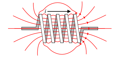
Inductors: constructed by making a coil out of a piece of a very long but low-resistance wire, so that the concentric magnetic field lines around the conductor add up inside the coil to form a powerful, coherent field (image). Because of the length of the wire needed, many small inductors will have a noticeable resistance - usually between 0.5 and 20 Ω.
Common inductor values in electronic circuits range from 1 µH to 470 mH or so. The usual symbol of an inductor is:

**Transformers:** constructed by pairing two inductors, typically wrapped around a common ferromagnetic core that guides and contains the electromagnetic field to improve performance. The interesting property of this arrangement is that changes in the current flowing through one of the inductors will generate a back electromotive force in the other, coupled coil. Coil turn ratio determines the ratio between the driving and the induced voltage, making transformers extremely useful for converting voltages (the law of conservation of energy ensures that transformers are not a free energy scheme: the power (V*I) must remain the same, and every increase in voltage reduces current capability proportionately). Another common use is galvanically isolating circuits for safety reasons - i.e., only magnetic coupling, but no direct charge flow pathways, would be maintained.
Their primary caveat is that they do not exhibit their trademark behavior when fed steady DC signals (once the core is saturated and peak magnetic field is attained, a significant winding current is admitted and largely goes to waste); and that optimum efficiency (often 95%+) is generally maintained over a fairly narrow range of AC frequencies (depending on the construction of the transformer). Low-frequency transformers, such as the ones used for 50-60 Hz mains signals, need large and heavy, slowly saturating cores; while high-frequency transformers can be much smaller.
The usual symbol is:
![]()
Sometimes, windings may have multiple taps, or additional windings can be provided as a feedback mechanism for building high voltage flyback transformers that exploit resonant frequencies of the ferrite core.
Electromechanical and optoelectronic devices [link]
There is a multitude of components that allow electronic circuits to interface with the outside world - from heat or radiation detectors, to various exotic display technologies, to thermal transfer devices. Listing them all is a futile task - but here's an overview of some of the most common components you may encounter:
Switches: one of the most rudimentary electromechanical devices, switches interrupt and close circuits in response to an externally applied force. These devices come in a wide variety of designs (rotary, paddle / toggle, rocker, pushbutton, slide, etc), and an even greater variety of sizes. Other than the power rating, their most important parameters are the number of actual switch positions, the number of "throws" (signal outputs the switch can alternate between - this must obviously be equal or smaller than the number of positions allowed), the number of "poles" (separate switching pathways put in a single package), and the type of switching action (sustained / latching or momentary; with momentary switches further divided between normally closed or normally open designs - "NC" and "NO").
Symbol for a single pole, single throw switch is shown on the left; a momentary, normally open switch is in the middle; and a single pole double throw is shown on the right:

Mechanical switches may also be operated by magnetic fields (Reed switch), gravity (mercury and ball-type tilt switches), liquid levels (float switches), and much more.
Simple actuators - electromagnets, speakers, solenoids, relays: as noted previously, electric currents flowing through properly oriented wires can induce strong, coherent magnetic fields; these magnetic fields may, in turn, interact with materials where electron spins are coherently aligned: permanent magnets and ferromagnetic / paramagnetic metals. An inductor designed with this in mind is called an electromagnet; the three most basic uses of electromagnets are speakers (where a diaphragm is being moved back and forth to create audible sound waves), solenoids (pushing or pulling a plunger - e.g., in car door locks or valves), and relays (mechanical switches operated by an electromagnet).
Generic electromagnets and solenoids are usually drawn as inductors, and merely annotated to indicate their intended function. The symbol of a loudspeaker is:

...and for relays, we tend to use:

Amusingly, relays and solenoids can be used as crude speakers when driven by audio-frequency signals.
**Motors and generators:** motors exploit the interaction of electromagnets and magnetic materials to put their output shaft in continuous rotary motion. This can be achieved by driving the coils directly with alternating sine wave currents (synchronous motors), by providing carefully timed voltage pulses (brushless and stepper motors), or with steady direct currents, mechanically switched by commutators (brushed motors).
This operating principle is reversible: when rotated by an external force, motors serve as generators, producing a voltage across their terminals. A striking demonstration of this is connecting the terminals of two similar, brushed DC motors together: rotating one of them will induce a voltage sufficient to turn the other.
The symbols used for motors are:

**Piezoelectric crystals:** certain materials tend to generate voltages in response to mechanical strain, and vice versa - contract or expand in response to applied fields or the currents flowing through them; in some settings, this action may in turn affect the applied voltage or admitted current, resulting in oscillating action.
These principles are used in a number of piezoelectric devices, the most common of which are crystal oscillators - where the crystal vibrates at a resonant frequency when subjected to an external current, similar to some capacitor-inductor arrangements we will discuss later on. Other applications use exotic, precision motors / actuators, piezoelectric transducers used to sense or generate soundwaves, pressure sensors, and so forth.
The usual symbol of a crystal oscillator is:

**Potentiometers:** manually adjustable resistors; can be constructed by placing a conductive wiper across a resistive substrate. Available as miniature board-mounted "trim pots" that need to be operated with a screwdriver, and are meant to be adjusted at assembly or servicing time; larger panel-mount devices with a knob or a slider used for interfacing with users; more expensive but precise multi-turn units of both flavors; and potentiometer-based position-, deflection-, or pressure-sensing components that provide the circuit with feedback about the position of monitored mechanical assemblies. In all cases, the usual symbol is something close to:

Potentiometers are usually not meant to conduct significant currents (and dissipate the resulting heat); therefore, using them requires some care.
Trimmer caps: manually adjustable capacitors; available only for small capacitances, usually controlled by gradually moving capacitor plates apart when a knob or a screw is rotated. Panel-mount devices were once very popular in radio frequency circuits to control the frequency of heterodyne receivers - but are now largely displaced by digital frequency generation that can be controlled with mechanically simpler input devices.
The symbol is analogous to that of a potentiometer - except that the "wiper" is not actually a terminal of the device:

**Incandescent lamps:** simple, well-known components that exploit the heat-driven light emission of a resistive metal wire placed under vacuum or in a low-pressure, inert gas (to prevent oxidation and minimize convection-based heat transfer). As the wire heats up, its resistance tends to rise - resulting in a self-limiting current flow that prevents the device from overheating and being destroyed within the (usually very generous) range of voltages it is designed for. Their primary downside is that they radiate most of their energy in the infrared range, which is not very desirable; and that they are slow to turn on and switch off, making them unsuitable for optical data signaling.
Lightbulbs are fairly unremarkable electrically, other than their interesting non-linear current characteristics: while the wire is cold, a significant current can flow, but only for a limited time. This sometimes results in non-conventional uses of lightbulbs in high-quality sine wave oscillators, such as the Wien bridge.
Incandescent lamp symbols:

**Light-emitting diodes:** certain types of semiconductor p-n junctions tend to emit light as electrons and holes recombine; LEDs are designed to exploit this phenomenon, instead of making use of the electrical characteristics of the junction itself. Unlike incandescent light bulbs, LEDs dissipate most of the energy as light, not heat - spare for some resistive losses in the semiconductor itself; and can be started and stopped very quickly.
These devices are more difficult to operate than lightbulbs, because they are very sensitive to the applied voltage - it must be enough to overcome the junction bias, but will result in a destructive current if off by as little as 0.2V. This is because diodes are only weakly conductive up until the potential of the junction is overcome - and shortly past that point, begin conducting like crazy. Current-limiting resistors or constant current supplies are commonly employed to prevent trouble.
Junction voltage drop is commonly in the 1.1 - 1.4V range for infrared diodes, 1.6 - 2.0V for red LEDs, 2.0 - 2.3V for yellow and orange, 2.2 - 2.8V for green, and 3.2 - 3.8V for blue, violet, white, and UV diodes. Commodity indicator LEDs are designed for currents between 5 and 30 mA. These parameters will vary from one device to another, and should always be confirmed with the datasheet.
In all other aspects, LEDs behave very much like a regular semiconductor diode, discussed in the next section. Their symbol is (arrow pointing in the direction of current flow - toward the negative pole of the supply):

Light sensors - photovoltaic cells, photoresistors, photodiodes: three additional uses of semiconductor materials where we don't really care about their electrical characteristics as such. Photovoltaic cells rely on a p-n junction to generate free charge carriers in response to photon excitation, and also to separate charges - so that an electromotive force is created across their terminals, forming a voltage source. Photodiodes work in a very similar way, but are used with an external voltage to achieve a current dependent on the amount of light shining on a reverse-biased junction. Finally, photoresistors are monolithic semiconductors where a higher number of photon-induced charge carriers promotes conduction; compared to photodiodes, they are much slower, but have other favorable characteristics, such as a very broad sensitivity range.
Their respective symbols:

**Microphones:** a variety of sound-sensitive devices (generally variable resistors, capacitors, or electromagnets) used to sample audio signals. The most common variety today are electret microphones that utilize an internal, permanently charged membrane to form an interesting type of a capacitor; but even a regular speaker and some vanilla capacitors exhibit some audio sensitivity.
The usual symbol of a microphone is:

Fuses: a variety of components designed to either irreversibly blow up (traditional fuses), toggle a mechanical switch, or just temporarily stop conducting (PPTC fuses) when the current flowing through them exceeds the desired value. Fuses are meant to protect more expensive or harder-to-service components from being affected when something goes wrong (e.g., a stray metal item shorts traces on the circuit board); and to prevent the circuit from overheating and starting a fire if the problem goes uncorrected.
The use of fuses in low-voltage, low-power consumer electronics is often a matter of a judgment call; but if the power supply can source significant currents, enough to blow a hole in the circuit board, adding a fuse may be a good idea.
"Proper" discrete semiconductors [link]
Diodes: a simple p-n junction that begins conducting well, but only in one direction, when an internal junction voltage (usually somewhere around 0.6 - 0.7V) is exceeded. It will not conduct in the opposite direction unless a much higher breakdown voltage is applied (this figure commonly lies between 20 and 1000V, although diodes with much smaller breakdown voltages can be manufactured). Two special types of diodes can be seen in electronic circuits along the "normal" ones: fast, low-threshold Schottky diodes used for small signal switching (with junction threshold of merely 0.2 - 0.4V); and Zener diodes with very precisely defined reverse breakdown voltage, often used as voltage references or voltage-limiting shunts that protect sensitive components.
The current-voltage curve for a typical diode may look roughly like this:

Past a certain forward or reverse voltage, any diode will happily attempt to conduct practically arbitrary currents. The interesting property of a diode (or any other p-n junction) is that while in this mode, the device will always maintain a potential close to that threshold voltage across its terminals: this electric field is necessary to keep the junction conductive, and the diode will develop an apparent resistance needed to maintain it. With higher currents, the measured voltage across the will increase subtly due to the resistance of the semiconductor material itself - but in most cases, this effect is not very pronounced (some Schottky diodes are an exception).
The symbol of a diode is an arrow pointing in the direction of current flow during forward-biased operation:

Some people use separate symbols for Zener (image) and Schottky (image) diodes, but you should certainly not bank on this.
Some of the most common general-purpose diodes are 1N4148 (rated for 1 A, 100V reverse voltage) and 1N400x series (1 A, assorted voltages from 50 to 1000V); BAT46 is a popular Schottky diode rated for 100 mA, with a low-current voltage drop of merely 0.25V; while 1N47xx is a family of popular Zener diodes with reverse breakdown voltages ranging from 3.3V to 200V.
**Field-effect transistors:** transistors are a very important class of semiconductor devices that, generally speaking, allow "weak" (low amplitude or high impedance) signals to control much greater currents flowing through the device - a sort of an electronically controlled potentiometer. They are primarily used as signal amplifiers, impedance converters, and digital switches.
MOSFETs - metal-oxide-semiconductor field effect transistors - are perhaps the most intuitive, if recent, variety. Three-terminal, enhancement mode, n-channel MOSFETs (the most common type) consist of a nominally non-conductive n-p-n junction. One of the terminals - called "drain" (D) - is connected to one of the n-type regions; "source" (S) terminal is connected to the p-type and the other n-type region; and "gate" (G) is placed across the p-type substrate, isolated with a very thin layer of glass; interestingly, this layer of glass is so thin that it is easily destroyed by electrostatic discharge - requiring all MOSFETs to be handled with care.
This arrangement of connections - shown below on the left - results in a normal p-n diode that allows conduction from source to drain - but no conduction the other way round; MOSFET transistors are operated with this junction reverse-biased - i.e., drain more positive than source in case of n-p-n devices.
The interesting part is that the isolated gate-source pathway through the p-type semiconductor acts as a small capacitor: applying a voltage higher than the source to the gate region will deposit a positive charge on the terminal, which pushes aways holes in the p-type semiconductor - and pulls free electrons from n-type terminals in, forming a junction-free conduction path (shown on the right):

There is some minimal gate voltage needed to cause a sufficient charge separation; this threshold voltage - VGS(TH) - depends on the geometry of the transistor, and generally ranges from 1 to 2V (but may be as high as 3-4V for high power devices).
MOSFET transistors allow very significant currents to be controlled by applying small, very high impedance signals to the gate terminal (there is virtually no gate-source current observed, and this "capacitor" retains the charge even after the source is disconnected); the resistance of the created conductive channel is proportional to the applied voltage, resulting in a transistor-specific two- or three-digit amplification factor (you shouldn't depend on its exact value, though).
Other common types of field-effect transistors are p-channel MOSFETs, which use p-n-p junctions, and switch on with a gate voltage is lower than the source voltage (and have slightly inferior electrical characteristics); four-terminal MOSFETs with no internal connection between the source and the middle semiconductor layer (the fourth terminal connected to this area is referred to as "body"), useful in some switching applications; less common depletion mode MOSFETs, which have a reversed operation, and are normally conductive until a field is applied to disrupt the channel; and somewhat simpler, depletion-only JFETs, which do not feature a glass insulator, and exhibit higher transconductance.
Symbols for n-channel and p-channel enhancement MOSFETs, and their on-by-default depletion mode equivalents, are shown below:

Interesting enhancement mode MOSFET transistors include 2N7000 (n-channel, 200 mA), NTD4858N (n-channel, 73A), or STP12PF06 (p-channel, 12A).
**Bipolar junction transistors:** BJTs are a bit more messy predecessor to FETs, allowing the current between their two terminals - "collector" (C) and "emitter" (E) - to be controlled by a smaller current flowing from the third terminal - "base" (B) - to the emitter.
BJTs consist of a nominally non-conductive junction, most commonly n-p-n - with the outer layers connected to the collector and emitter terminals, and a very thin p-type layer sandwiched in between connected to the base terminal (see image below, left).
In normal operation, collector is connected to a more positive region, and emitter is more negative; in this configuration, the B-C junction is reverse biased and does not conduct. When a small current between the base and the collector is applied, however, the B-E junction depletion layer collapses; and because of how thin the base layer is, the depletion layer on the B-C junction is also compromised. High-velocity electrons that are accelerated by the B-E voltage and inject from the emitter into the p-type semiconductor will easily make it to the collector layer - and a significant current will flow (a device-specific two- or three-digit current amplification will be seen, the exact value of which is - again - not to be relied upon):

Bipolar junction transistors with n-p-n arrangements are, somewhat unimaginatively, called NPN. Their p-n-p counterparts (PNP) operate with the emitter being more positive, and conduct when a current flows from the emitter to the base. The symbols of NPN and PNP transistors are:

All bipolar transistors are more hairy than MOSFETs, for a couple of reasons. Firstly, they can't be driven by extremely high impedance signals, because some small base current must flow to enable conduction. Secondly, their diode junctions do not disappear fully when the transistor is conducting, resulting in an unavoidable voltage drop (VCE) across the device - usually between 0.1V and 0.4V when the transistor is saturated (i.e., further increases of base current have no effect). Similarly to MOSFETs, there is also a minimum base-emitter voltage required to overcome the potential of the BE junction (VBE), usually in the 0.6V - 0.8V range.
The three most common BJTs are 2N3904 (NPN, 200 mA), PN2222A (NPN, 1A), and 2N3906 (PNP, 200 mA). Higher-rated variants, such as FJN965 and FJC1386 (NPN and PNP, 5A) can also be found, but MOSFETs are now being used almost exclusively in power applications.
"Derived" transistors: a variety of more exotic transistor arrangements exists. Thyristors (also known as silicon controlled rectifiers, SCRs) are four-layer semiconductors that behave like latching transistors - i.e., keep conducting even after the base current stops; this effect can be also approximated by two discrete transistors (image). Darlington transistor is a pair of two NPN or PNP transistors stacked to achieve a much higher current gain; and Sziklai pair is its heterogeneous (NPN+PNP) counterpart. Field effect transistors with multiple "competing" gate electrodes can also be seen, and are useful in signal mixing.
With the operation of transistors explained, it's good to additionally mention phototransistors - optoelectronic devices that operate very much like photodiodes, but feature internal gain; and optointerrupers - LED-phototransistor pairs mounted in a common enclosure, used for reflective or transmissive (slot) sensing in a variety of mechanical applications.
Analog circuits [link]
Now that we have the basic characteristics of electronic circuits, and the common components, sorted out, it's time to see what it's good for - starting with traditional, analog circuitry.
Components in parallel and in series [link]
When considering the behavior of real-world circuits, it is often essential to understand the actual resistance, capacitance, or inductance of signal pathways that may consist of more than one discrete component. Thankfully, this is fairly simple.
As should be fairly obvious, several resistors placed in series will have an equivalent resistance equal to the sum of all individual resistances:
Requiv = R1 \+ R2 \+ R3 \+ ...
Resistors placed in parallel, on the other hand, have an equivalent resistance equal to the inverse of the sum of their inverse resistances:
Requiv = 1 / (1/R1 \+ 1/R2 \+ 1/R3 \+ ...)
This latter calculation is somewhat cumbersome, but for simplicity, it's good to remember that any number of identical resistors in parallel will have an equivalent resistance equal to R/count, and the power rating will increase accordingly; and that if and if one of the resistors in parallel has a resistance several orders of magnitude lower than the rest, the resistances and power ratings of the remaining resistors may often be safely ignored altogether.
Exactly the same rules apply to the inductance and power ratings of inductors; and the voltage and current capability of voltage supplies.
Capacitors, on the other hand, behave differently; in parallel, their capacitance increases - and in series, drops. This is easy to understand by considering that several identical capacitors in series are essentially equivalent to a single capacitor with a thicker layer of a dielectric (the fact that these is a piece of conductor in the middle is of no significance for its operation) - and therefore, a lower ability to cancel out the electric field generated by unbalanced charges deposited on the plates; consequently, several capacitors in parallel resemble one capacitor with a larger plate surface area.
Thevenin's theorem is a sometimes useful analytic tool, too: it gives a method for replacing any network of resistors, voltage sources, and current sources, with a single voltage source and a single resistor. You do not have to memorize it, but it's good to be aware of this possibility.
Resistors as current limiters [link]
Ohm's law states that when a particular voltage is applied across resistor terminals, only a current proportional to this voltage, and inversely proportional to resistance, will be allowed to flow: I = V/R. This brings us to the simplest application of resistors:

In this circuit, a 9V battery is supposed to light up a red LED. From the datasheet, we know that the LED, when supplied with 1.9V, sinks exactly 20 mA. Equipped with this knowledge, we can calculate that at this exact point, its internal resistance is 95 Ω. Unfortunately, diodes have a highly non-linear I-V curve - so when we connect 9V, its resistance will suddenly drop, several amps will be allowed flow through the junction; and the whole thing could - nay, will - catch fire.
Thankfully, we can prevent this current from flowing in a very simple way. First, we need to find an equivalent resistor that, when placed across the terminals of our 9V battery, would conduct just 20 mA. Then, we can subtract 95 Ω - and get the resistance that needs to be placed in series with the diode to achieve the same result:
Requiv = 9V / 0.02A = 450 Ω
R = Requiv \- 95 Ω = 355 Ω
The voltage drop across this resistor would be 0.02A * 355 Ω = 7.1V - leaving exactly 1.9V for the diode.
To build this circuit in practice, we can safely use use the nearest "preferred" resistor value, 330 Ω (which would actually allow 21.5 mA to flow through the device - well within the safety limits of most components).
In this particular use, the power dissipated by the resistor (P = I²R) will also be negligible - around 1/8 watt; for higher currents, the amount of dissipated heat goes through the roof pretty quickly, though - and therefore, resistor-based current limiters are useful only in low-power uses. This device is also not a perfect current limiter: if the apparent resistance of the driven device drops during normal operation, a more significant current will be allowed to flow. In both these cases, a more sophisticated, active circuit - implementing a "real" current source - is necessary instead.
It is also important not to treat a current-limiting resistor as a way to reduce voltage: note that with the load (LED) disconnected, no current will flow through the resistor - and therefore, there will be no voltage drop across its terminals (V = IR); the output voltage of the circuit will be identical to that of the supply - and will drop quickly, but thanks to parasitic capacitances not instantaneously, when the load is connected again.
Resistors as voltage dividers [link]
In the following circuit, with the lightbulb disconnected, the current flowing through the circuit will obviously be equal to Vsupply / (R1 \+ R2):

From this, we can calculate the voltage measurable across the terminals of R2:
VBA = IR2 = Vsupply * (R2 / (R1 \+ R2))
If R1 is equal to R2, the voltage across B and A will be 1/2 Vsupply; if R2 is twice the R1, the B-A voltage will be 2/3 Vsupply; and so forth - it's a simple matter of the ratio of resistances, independent of the absolute values of the resistors (and the resulting current flow). The circuit simply divides supply voltage by a desired factor - and in this, lies its utility.
This divider is not a perfect voltage source, however: when you connect any resistive load (R3) between A and B - for example, the lightbulb shown on the schematic - it will introduce a new resistance parallel with R2. You may remember that this is equivalent to replacing R2 with a new resistor:
Rnew = 1 / (1/R2 \+ 1/R3)
When the expected range of R3 values to be seen by the circuit is much higher than the value of R2, the effect is negligible - but when R2 and R3 are in the same league, the resulting voltage drop may become significant. Therefore, the resistors need to be picked with the expected loads - and the acceptable voltage swings - in mind. In many cases, this is not a big deal; but when driving power-hungry devices, R1 and R2 may have to be so low, that the resulting quiescent current through them would render the arrangement completely impractical.
In other words, practical resistor-based voltage dividers can be considered medium to high impedance sources, and should not be driving low impedance loads.
Capacitors for energy storage [link]
Consider the following circuit:

When SW1 is toggled, the capacitor will gradually charge through a resistor. Without this resistor, the time it takes for it to charge would be theoretically zero - and in practice, would be limited by poorly predictable factors such as the internal resistance of the device, or impedance of the power supply; but with a resistor, At t = 5RC, the capacitor will be more than 99% charged, with almost no current flowing - and a voltage equivalent to that of the power source will be present across its terminals.
What happens if we open SW1 and close SW2 at that point? A current will be allowed to flow through the lightbulb, discharging the capacitor in a familiar manner, with discharge time governed by capacitance and the equivalent resistance of the driven device. The lightbulb will be getting more and more dim as the voltage across the capacitor drops; depending on its exact characteristics, somewhere around t = 2RbulbC (15% of supply voltage), it will probably go completely dark.
A more interesting case is what happens when both switches are switched on at the same time: assuming the non-linearity of the lightbulb is negligible (which is fair if the capacitor is large enough), initially, the capacitor will offer a low-impedance path, with very little current flowing through the bulb; but as the charge builds up, the voltage across its terminals will begin to rise - and more current will flow through the bulb. The capacitor will never charge past the voltage across the terminals of the lightbulb (which can be calculated from the lightbulb's resistance, as per Ohm's law) - and will discharge through it when SW1 is opened. In effect, this circuit gradually fades in and fades out the light when the switch is toggled.
The action of a capacitor in parallel with a load appears to be reminiscent to the behavior of a series inductor. There is one key difference inductors oppose changes in current for a longer time when the current is higher; whereas a capacitor has a more pronounced effect when the current that charges or discharges it is lower; were we to eliminate the upstream resistance, the capacitor would charge instantaneously.
Passive resistor-capacitor (RC) signal filters [link]
A variety of resistor-capacitor-inductor arrangements can be used to form circuits with interesting frequency response characteristics. Perhaps the the simplest case are the following two RC designs:

In the circuit shown on the left, the capacitor will be charged or discharged by any (sufficiently low-impedance) input signal at a rate controlled solely by the resistor; with the capacitor discharged, the output voltage will start at zero, and will begin approaching the input voltage only if the signal is applied for long enough (3RC or so). This has an interesting consequence: when the signal is a sine wave of a very low frequency, much lower than the capacitor charge time - the output voltage will, with a slight lag (phase shift), simply follow the input. As the frequency increases, however, the signal will get more and more attenuated - and the phase shift will become greater - as the source can't charge or discharge the capacitor quickly enough. This circuit is, therefore, a simple, passive low-pass filter.
An example of a linear response curve for this filter may look like this:

A logarithmic plot over a larger scale of frequencies is perhaps more informative, though:

What about the second circuit shown on the earlier image? As it turns out, it exhibits exactly the opposite behavior: the capacitor prevents the flow of any DC currents - or the transfer of DC voltages - but when a negative voltage is applied to one of the plates, electrons will be pushed away from the other, and vice versa. If the resulting flow of charges is slow enough, they will simply drain through the resistor; but if the rate of change is very high, the resistor will limit the current, and develop a substantial, momentary voltage difference across its terminals. This circuit passes higher frequency sine wave signals largely unaltered, but attenuates slow-changing sine waves - a high-pass filter.
It is customary to describe these circuits in terms of their cutoff frequency - a sine wave frequency at which the signal is attenuated to half its power (or, if you recall from the section on decibels, 0.7 of its input voltage). This point can be calculated as:
fcutoff = 1 / (2 * π * RC)
For any sine wave frequency f, amplitude multiplier (g) for the transferred signal is ideally:
glowpass = 1 / √(1 + (f / fcutoff)²)
ghighpass = (f / fcutoff) / √(1 + (f / fcutoff)²)
As should be evident, there are many resistor-capacitor combinations that yield the same R*C product, and therefore, the same frequency response. The difference is that the smaller the resistor, and the larger the capacitor, the lower output impedance the filter will have - but the more power it will keep wasting, and the lower the impedance of the driving signal source would need to be to avoid distortion. The usual procedure, then, is to select R one or two orders of magnitude smaller than the impedance of the driven load - and calculate the right C for the required cutoff frequency.
Note that these circuits work as expected only for sine waves (and in such a case, will output a sine wave, too). When fed with other waveforms, including square, triangle, or sawtooth signals, they will behave differently - and introduce interesting artifacts of their own. For example, for square waves (shown in green), the output of a low-pass filter below its cutoff frequency (i.e., transmissive state) may be:

...and well over the cutoff frequency, it may begin to resemble a sawtooth wave, with an amplitude decreasing in function of frequency:

The output for a low-pass filter is essentially proportional to how long the signal stayed in a particular state; for this reason, it is sometimes called an integrator.
The behavior of a high-pass filter fed with a square wave is perhaps even more interesting - with a voltage proportional to the rate of change of the input signal (hence the nickname: differentiator). Above the cut-off frequency (i.e., in its transmissive state), the output may look like this:

...while well below the cut-off frequency, it may begin to resemble:

Note that in both cases, the high-pass filter peak output amplitude is nearly twice the input amplitude; only the average power of the signal (RMS) is affected when the input frequency changes.
The ability to spot these waveforms is actually extremely useful when debugging digital circuits, where square wave signals are used extensively. An unexpected low-pass filter distortion seen in a digital signal is usually indicative of excessive capacitance of the signal path, perhaps because the connection is too long, or runs too close to others; while a high-pass pattern may indicate a broken trace or cut wire, forming an unwelcome capacitor in series with the source of the signal.
Low-pass and high-pass filters can be cascaded to form band-pass or band-stop filters; identical filters can also be stacked to achieve a steeper response curve (n-th order filters, with gn frequency transmission function). That said, this process has its limits: every stage needs to have an impedance much lower than the subsequent stage it is driving, which quickly leads to impractical or very inefficient arrangements; and every stage attenuates the desired signal to some extent, inevitably reducing signal-to-noise ratio.
Inductors in signal filters (RL and RLC circuits) [link]
Inductors can replace capacitors in RC filters, reversing their operation: an RL filter with the same topology as an RC low-pass filter will act as a high-pass filter, and vice versa; the reason for this should be fairly evident. The cutoff frequency for RL filters is:
fcutoff = R / (2 * π * L)
In other aspects, the signal response of RL filters is essentially identical to that of their RC counterparts.
A more interesting class of circuits are RLC arrangements where the capacitor is "fighting" the inductor, and the resistor moderates the maximum current supplied to them:

The circuit on the left is, essentially, a band-pass filter: the capacitor needs the signal to change slowly enough to charge it up to an appreciable level - and above this frequency, serves as a shunt; but when the current is not changing fast enough, the inductor will begin conducting and will discharge the capacitor. This can be thought of as a combination of an RC low-pass and an RL high-pass filter, with a peak bandpass frequency of:
fpeak = 1 / (2 * π * √(LC))
...and a bandwidth between 3dB attenuation points of:
BW = R / (2 * π * L)
The effect of adjusting bandwidth by changing the value of R is shown below:


In practice, the optimal way to design an RLC band-pass filter is to pick R to achieve the desired output impedance; continue with L for the desired bandwidth; and finally, C to set the center frequency.
As to the other circuit shown earlier, on the right - it is a band-stop filter: the coil conducts well only below a certain frequency, and the capacitor conducts well only above another; the signal will be shunted to the ground most efficiently in between the frequencies. The only difference is that the blocked bandwidth is given as:
BW = 1 / (2 * π * RC)
Many other RLC circuits can be designed, although these two approaches are most useful when easily understood dependence on source and load impedances is required. As with RC and RL filters, the gotcha with RLC circuits is that in signal processing, the impedance of the driven load must be significantly higher than that of the signal source and the series resistor in the circuit - or else, distortion will appear.
Transistors as switches [link]
Transistors differ from passive electronic circuits because of their ability to introduce gain - that is, turn low-amplitude voltage signals into high-amplitude ones, or high-impedance signals into low-impedance ones. For now, let's neglect their more complex response characteristics, and focus on a very simple, binary switching application - using a potentially low voltage or high impedance signal to control a power-hungry or high-voltage load:
![]()
The circuits in the A column show common, proper transistor switch arrangements for NPN, PNP, and MOSFET n-channel enhancement mode transistors - known as "common emitter" (BJT) or "common drain" (FET). In NPN and PNP circuits, note the use of a resistor to limit the base-emitter current: the current flowing through this path must be controlled, because the corresponding junction is essentially a normal, forward-biased diode - and will conduct as much current as you supply, possibly destroying the transistor in the process (and certainly making it misbehave).
Bipolar transistors have a device-specific current gain ratio, usually labeled as hFE in the datasheets. Relying on this intrinsic gain is usually not a good idea for production-grade circuits, as the parameter can change significantly at a whim - but by looking at its general order of magnitude, you can see what input impedance would be appropriate. For example, if hFE = 100, and the load requires a current of 500 mA, at least 5 mA of base current should be supplied (supplying more will be wasteful and may lower switching speed, but the margins here are pretty wide). Base-collector junction voltage is probably around 0.7V, so with a 5V supply, a voltage of 4.3V would be present across the resistor; from Ohm's law, and with an ample safety margin, a 680 Ω resistor would be a good bet.
Because of the need to limit current, the NPN arrangement shown in column B is universally a bad idea: it will likely destroy the transistor; its PNP equivalent is equally disastrous.
The MOSFET transistor shown in column A generally does not require a resistor, at least at low signal frequencies, because it does not allow any appreciably long-lived current to flow through the gate (at very high frequencies, the small but non-zero gate-source capacitance becomes a factor, though). It does, however, need bipolar switching: if you simply apply a positive voltage to the gate, and then disconnect it - the gate-source "capacitor" will stay charged, and the transistor will continue conducting for a longer while (dependent on humidity, handling, etc); even after this charge disappears, a new one can be easily accumulated due to further handling, parasitic coupling, and so forth. This is why the MOSFET circuit shown in column B is always a bad idea, too. It can be alternatively fixed by adding a large pull-down resistor from the gate to the ground, to dissipate the deposited charge when the switch is opened, but at the expense of lowering input impedance.
Column C shows another arrangement that is not universally problematic, but should be avoided in switching where possible - and is all-too-common in hobbyist work: loading the emitter (BJT) or drain (MOSFET) - a configuration known as "common collector" or "common source". The problem with this is that all real-world loads will develop some voltage across them in normal operation; this raises the emitter or source voltage accordingly - perhaps close to, or even above, the driving base / gate voltage. This causes the switching to be far more erratic, especially with inductive loads. There are uses where this arrangement makes sense - but switching is not one of them.
In all cases, the driving voltage applied to the base (or gate) must be high enough to trigger the transistor; that is, at least 0.6V in BJT, and at least 1-2V for most MOSFETs. At this point, the transistor just barely begins conducting - so ideally, in switching applications, Vin should be comfortably higher. In BJTs, around 1V ("base saturation voltage") is sufficient to achieve a full range of meaningful base currents; in MOSFETs, resistance becomes negligible usually around 3.8V.
The drawback of the transistor switches shown earlier is that they work in a manner similar to a single-pole switch: they can connect the load to the ground (NPN, n-channel MOSFET) or to the supply rail (PNP, p-channel MOSFET), or simply leave it in open circuit state. When turning on a lightbulb or a LED, this is not a problem - but when driving inductive or capacitive loads (including the gates of MOSFET transistors), or encoding information as voltage levels, it may be more desirable to offer two-pole operation, where the output can be switched between two low-impedance rails. The simplest way to do so is a push-pull circuit that uses complementary transistors to do the job:
![]()
When the input voltage is close to 0V, the bottom transistor will not conduct, but the upper one will. When the voltage is close to the positive rail, the situation will reverse. When the voltage is somewhere in between, though, both transistors may end up conducting, shorting the circuit - so caution must be exercised; this problem can be controlled by carefully biasing bases / gates using resistor-based voltage dividers, but it may affect switching performance.
Also note that the upper transistor, connected to the positive rail, is PNP or p-type MOSFET; and the bottom one, grounded, is NPN or n-type MOSFET. This ensures that both transistors are operating in common emitter / common source mode, suitable for switching. Reversing the order of these transistors may lead to trouble for the reasons discussed above; the same goes for trying to use two identical transistors, just hooked up in opposite ways.
What else? Ah, inductive loads, such as motors, deserve some special attention: when a current supplied to an inductor is suddenly cut off, the energy stored in the collapsing magnetic field will try to keep the charge carriers in motion; and if this proves to be impossible, a very brief (nanoseconds) but significant (up to kilovolts) electromotive force will be created. This phenomenon is responsible for the sparking commonly seen in low-voltage brushed motors or toggle switches.
In some cases, this transient voltage may damage sensitive transistors in the vicinity - for example, compromising the gate insulator in MOSFETs, or simply overheating and vaporizing a part of the junction. To prevent this, a reverse-biased, normally non-conductive diode with a sufficient power rating is sometimes placed across such loads:
![]()
The function of this diode is to begin conducting, due to the breakdown effect, when the terminal voltage gets dangerously high. To be fair: in most cases, such a diode is not necessary - because switching is never perfectly instantaneous, inductors are never ideal, and the parasitic inductances, capacitances, and resistances of the circuit will dissipate the energy before it gets near a fragile semiconductor - but these factors are not necessarily predictable, so especially with more significant inductances, it is simply a good engineering practice... after all, a suitable diode usually costs just several cents.
Transistors as voltage followers and amplifiers [link]
The previous section discusses the use of transistors as binary switches operated in their saturation region - that is, the point where the resistance is minimal, and the admitted current is at its peak. Another important and more subtle use of these semiconductor devices is amplification, however - modulating output signals in relation to input voltage or current.
Perhaps the most rudimentary, but surprisingly not the most interesting application of a transistor as an amplifier is the previously discussed common emitter / common source setup:
![]()
The current supplied to the load remains in some clear relation to the input current (BJT) or voltage (MOSFET), for as long as the input remains in the "linear" range for the device. Alas, the exact input-output ratio (hfe) is hard to predict - the parameter changes from one batch of transistors to another, and is also highly influenced by factors such as voltage or temperature.
You can use this arrangement to adjust the speed of a motor with a small potentiometer, or perform other non-critical tasks of this nature; but for anything that requires precision and repeatability, this is just poor engineering: people should be able to substitute transistors used in your circuit with comparable alternatives, or use a 5% accuracy input resistor, and still have it work.
So, instead, let's have a look at a more useful, if modest, type of a simple transistor circuit: a voltage follower, also known as a buffer. In this "common collector" / "common drain" device, output voltage simply follows the input voltage 1:1 (a setup known as "unity gain"); its utility is that a high-impedance input can be "converted" in a low-impedance, high current capability output:

To understand why the circuit shown in the first column works as advertised (and why no base resistor is needed), it is important to recall that an NPN transistor will only admit any base-emitter current (and therefore, collector-emitter current) when the voltage difference between the base and the emitter is sufficient to overcome the potential of the internal p-n diode junction (circa 0.6V). In other words, the transistor will only try to conduct just enough current - bulk of it through the collector-emitter pathway - to keep the voltage across R1 (and therefore, at Vout) at exactly Vin - 0.6.
Ohm's law states that the current needed to develop a particular voltage across the resistor will be proportional to the desired voltage, and inversely proportional to resistance; if R1 is reasonable, so is the collector-emitter current. The base-emitter voltage is kept near the diode conduction threshold, so the current flowing through this path is also very low and self-limiting (and naturally, avoided entirely in MOSFETs).
This circuit has some drawbacks, though. For starters, there is a voltage offset present between the input and the output; for inputs between 0 and 0.6V, the output will be simply clipped at 0V. Connecting the emitter to a negative voltage at least 0.6V higher than the lowest signal voltage is a potential solution to the clipping problem - but it may be impractical in some settings. Another simple (but imperfect) way to prevent this problem begins with AC coupling - the introduction of a series capacitor that prevents any steady DC currents or voltage levels from propagating through it, but allows time-varying signals to induce a voltage across it. Once this is done, a simple resistor-based voltage divider can be used to add an arbitrary bias to the resulting AC signal, for example to add +3V. This circuit is shown in column B above. Its key flaw is evident once we recognize the capacitor and the resistors as a high-pass filter: this filter inevitably attenuates sufficiently low frequencies and DC voltage drifts. In many cases, this is not a big deal - the capacitor and the resistors can be selected with the interesting range of frequencies in mind; but fundamentally, the follower is no longer maintaining direct relationship between input and output voltages - and merely between their rates of change.
Bias and clipping aside, another problem with simple voltage followers that they can only source, but not drain, significant currents. This is more of a deal here with voltage followers than it is with switches: consider driving a capacitor as a load, connected across the "out" node and the ground. When Vin is 6V, the capacitor will very quickly charge to 5.4V, as a significant current flows through the transistor. Alas, when Vin later drops to 2V, Vout will stay at 5.4V - and because emitter voltage is now higher than base voltage, the transistor will not conduct. The capacitor will slowly discharge through R1 - but R1 can't be arbitrarily low (the quiescent current flowing at all times through the follower would be rather impractical if we go too far, and input loading would increase, too). Until then, the follower will not be following the input voltage at all.
A simple way to fix it is to have the input signal drive two complementary transistors at the same time, placed on both sides of the "out" node; this is known as a push-pull amplifier. This arrangement still suffers from the 0.6V bias - but this time, it can be solved more neatly than with AC coupling: by biasing both transistors into symmetrical, slight conduction when Vin is at the mid-point - and simply relying on the input signal to swing the ratio. This bias-compensated, DC-coupled voltage follower is shown in column C above; try to think for a moment about how it works in practice - and observe that the arrangement of transistors is opposite to that in a push-pull switch.
Voltage followers may sound boring, but they are immensely useful in electronic circuits; for example, they can be used to bridge a significant number of RLC band-pass or band-stop filters, or to convert very faint high-impedance currents from external sensors into outputs suitable for other circuitry. Still, you are probably wondering about a different task more commonly associated with amplifiers: increasing the amplitude of a weak signal. When faced with this problem, almost all hobbyists immediately think of the intuitive, hfe-dependent circuit discussed initially in this section - but there is a better way:
![]()
Let's see how this works: the transistor will seek to supply such a current to R2 to achieve a voltage matching Vin - 0.6V across this resistor (assuming for a while that R1 permits so); as per Ohm's law, I = (Vin \- 0.6) / R2. This flow of current, however, will also create a voltage across R1: V = IR1 = (Vin \- 0.6) * R1 / R2. In other words, Vout will be amplified by R1/R2 - with no dependency on hfe! Note that in this particular circuit, the output signal is inverted (i.e., is at supply voltage when Vin is 0V); that problem is obviously easy to correct if necessary - for example by adding a second stage with R1 = R2.
An interesting extension of this simple concept is a differential amplifier - a device that compares two voltages, and outputs the difference between them, multiplied by some factor:

This circuit essentially consists of two conjoined voltage amplifiers from the previous example. When their base voltages are identical, they agree on what the voltage of their emitters should be; each will contribute 50% of the current that needs to flow through R2 to produce that result. When Vin2 is higher than Vin1, the right transistor will insist on getting the emitter voltage to a point where the left one no longer conducts - and so, the current flowing through the right R1 (and the associated voltage drop) will increase.
As to the point of it all: differential amplifiers are extremely useful for subtracting RF interference or removing or adding bias voltages from input signals without the need to use AC coupling.
Naturally, a wide range of refinements to these basic designs is known today - say, to improve linearity, bandwidth, or to compensate for temperature variations. You will also probably stumble upon many other, more exotic transistor circuits not covered here - such as, for example, current mirrors or common base / common gate amplifiers - but you can probably figure them out by now.
Diodes as shunts and regulators [link]
The tendency for diodes to maintain a precise voltage drop across their terminals is often exploited to provide precise voltage references in a circuit. Forward-biased diodes, with their 0.2 - 0.7V voltage drops, are usually less useful; but reverse-biased Zener diodes are a wholly different story.
The most unsophisticated use of a diode is a shunt; shunts may be placed across the terminals of high-impedance, low-precision signal sources to trim the voltage to a particular level; or to suppress transient voltage spikes caused by inductors, electrostatic discharge, or even lightning strikes (using a specialized varistor diode). The usual "dumb" shunt circuit is:

While very useful for controlling high-impedance signals, the diode simply serves as a "crowbar" across the supply terminals - and therefore, for input voltage sources that can source a significant current, this arrangement gets dangerously inefficient; a resistor can be used to limit supply current, of course - but this simply takes you back to the high-impedance scenario - not very useful for, say, driving motors.
A simple modification of this approach is to combine a voltage follower with a reverse-biased diode; the follower will then always attempt to output a voltage equivalent to diode breakdown voltage, minus the inherent drop across the follower itself:

The resistor on diode side should be selected to limit the current through the diode to a reasonable value, so that it has an opportunity to develop a voltage across its terminals in the first place, but so that it does not waste too much power. The spec for the diode usually gives a "rated reverse current" or IZT figure, corresponding to the rated reverse voltage; in most cases, several milliamps is ideal.
The previously discussed modifications of the voltage follower circuit - to allow adjustable voltage amplification and push-pull operation - are just as applicable to this regulator. The key advantage of this design is that unlike a resistor-based voltage divider, it does not waste tons of energy - and achieves much better regulation over a wide range of possible loads.
Diodes are also commonly used to build constant-current sources, such as this circuit: this arrangement will admit only as much current as needed to create a particular voltage across the constant "sense" resistor, R2, regardless of the potentially variable voltage drop seen across the connected load.
Diodes as rectifiers, DC restorers, and voltage multipliers [link]
Forward-biased diodes serve a number of useful functions of their own. Let's begin with basic rectifiers - devices used to extract the absolute value of a voltage that swings both ways from the 0V rail:

The behavior of the first circuit - known as a half-wave rectifier - should be fairly clear: the diode conducts, and therefore creates a voltage across the resistor (a dummy load), only if the first input is more positive than the other; in this circuit, diode breakdown voltage is selected high enough not to interfere with this process. The second circuit - a bridge or full-wave rectifier - is a bit more clever, but also easy to follow: opposing pairs of diodes are used to select the more positive or negative out of two input leads, and always produce a particular output polarity.
Why is this useful? Well, the input AC signal, which (if symmetrical and steady) has an average DC voltage of 0V; if you connect a large capacitor to it, its average charge will also be 0V, and all the energy used for charging will be wasted. The output waveform from a rectifier has non-zero average DC voltage, though - corresponding to the amplitude of the input signal (shown below in green in the graph below). This output can be then used to construct rudimentary approximations of DC voltages using just a single cap (red is the voltage across the load):

This circuit, common in mains-powered supplies, should be fairly easy to understand: a low impedance AC signal is rectified, and then used to instantaneously charge a capacitor; the capacitor will only be charged if its terminal voltage is below that of the rectified waveform, too - at all other times, the diodes are reverse-biased and do not conduct.
As long as the rate at which this capacitor is discharged by a load is much lower than the rate at which it can be recharged, the output signal is a close approximation of a DC supply; the larger the capacitor, the smoother the DC output is.
A variation of this circuit is called an envelope follower: in this case, the resistor and the capacitor are matched to form a low-pass filter that "masks out" a high-frequency carrier, but passes through a lower frequency envelope (in this use, no significant output loading is present). Envelope followers are commonly used to separate modulated audio signals from high-frequency carrier signals used in radio transmission:

Another interesting use of a diode is DC restoration - a process where a symmetrical AC signal is offset so that the flow of current becomes unidirectional - but that the waveform is not distorted otherwise:

This arrangement may be a bit tricky to understand: the key point is that when a negative voltage -X is applied to a reasonably large capacitor by a low-impedance source, the internal electric field will induce a similar voltage on its other terminal (i.e., any external electromotive force will propagate through the dielectric medium when no existing charge is deposited on its plates) - and this will prompt the diode to begin conducting, allowing the current to flow, charging the capacitor to -X volts, and keeping the potential between output terminals close to 0V.
When the input voltage then swings to +X some time later, the resulting electromagnetic field propagates a 2X voltage swing across the capacitor; but this time, the reverse-biased diode will not conduct, and will prevent the already deposited charge from exiting the capacitor (except through any externally connected load). The subsequent -2X swing will bring the output voltage close to 0V, then back to 2X, and so on.
Naturally, to avoid surprises, the capacitor must be large enough not to form such a high-pass filter with the load (or the always weakly conductive diode) as to substantially attenuate the input AC signal.
A really interesting combination of the previous two circuits is a diode-based voltage multiplier: the output of a DC restorer can be used to gradually charge a capacitor to the peak output voltage, which is then used as a ground reference for another DC restorer. The behavior is illustrated below, with a 5V amplitude AC signal as the input:

Voila - we turned an AC signal with peak-to-peak voltage of 10V into a DC signal with peak voltage of 20V. The multiplier can be stacked, although diode and capacitor leakage currents and other losses put some constraints on its scalability.
Transistor-based oscillators [link]
Resistors, inductors, capacitors, and piezoelectric crystals may be arranged into many types of resonant circuits that will generate alternating voltages; one of the simplest examples is just a capacitor and an inductor in a closed, series loop: a previously charged capacitor will discharge through the inductor; the resulting magnetic field will then collapse and induce a current that re-charges the capacitor - and so forth (the resonant frequency is 1 / (2 * π * √(LC))).
The only problem with such circuits is that they lose energy and stop oscillating appreciably after, at best, several dozen swings: some of the magnetic field will be inevitably dissipated, and so will some of the current due to real-world resistances and capacitor leakage. Transistors come to the rescue, however: by detecting a particular state of the oscillator and supplying additional energy - a well-timed push - the oscillation can be sustained indefinitely. Simple transistor LC circuits, such as Hartley, Armstrong, or Clapp oscillators make use of this operating principle.
To illustrate the basic operation of many types of oscillators, let's have a look at this simple, RC-only square wave oscillator (aka "multivibrator"):

The circuit consists of two identical MOSFET switches driving small resistive loads equipped with an output tap; this tap will be at Vsupply when the MOSFET is off, and close to 0V when fully conducting. This output voltage is then AC coupled through a capacitor (C = 1 µF), biased to ½ Vsupply using a voltage divider consisting of two large (R = 100k) resistors - and finally employed to drive the gate of a complementary MOSFET.
When the circuit is initially turned on, the MOSFET on the right will turn on first, as its gate is driven through a slightly smaller resistor. This will cause it to pull the output down, and create a negative voltage across the capacitor driving the left transistor. This negative voltage will prevent that MOSFET from turning on until the charge is dissipated through the voltage divider (which takes time proportional to the capacitances and resistances involved) - and the gate is positive enough again.
At this point, the left transistor will turn on, and create a negative voltage on the gate of the other MOSFET, turning it off for a while. The cycle will repeat indefinitely, generating a square wave (the frequency of which is approximately 0.72 / RC - or about 7 Hz in this particular case).
Analog integrated circuits [link]
In addition to discrete components, a wide selection of integrated circuits is available today. These highly miniaturized, modular building blocks consist from anywhere from several to hundreds of millions individual components packed on a single die, usually produced by the means of photolithography. Some of the most popular varieties of analog ICs are:
Transistor drivers: one of the most rudimentary classes of integrated circuits, these chips consists of a modest number of individual transistors, often with protective resistors and diodes, to be used as line drivers (i.e., impedance converters). One of the most common devices in this category is ULN2003A, a set of six Darlington transistors; more complex devices with push-pull control or low-distortion signal switching, also exist, and are just as easy to follow.
**Operational amplifiers:** advanced, differential push-pull voltage amplifiers with very high impedances (sometimes using JFET or MOSFET transistors), variable gain, temperature and supply voltage compensation, internal biasing, voltage drop compensation, and so forth - essentially designed to approximate a perfect amplifier within a fairly wide range of operating conditions. Op-amps usually accept two inputs (non-inverting, marked as "+"; and inverting, marked as "-") and have one output. When the input voltages are identical, the output voltage is exactly 50% of the supply range; and when the voltages differ, the difference will be amplified and output as a swing toward the negative or the positive supply rail. The "default" amplification of an op-amp is very high and not necessarily well-defined - but can be controlled very precisely by adding a negative feedback pathway between the output and the inverting input.
The most common use of an op-amp is probably building a "normal" single-input amplifier; the amplification is then equal to the ratio of the feedback resistor (R1) to the impedance of the other signal supplied the inverting input (R2, generally in the 10 - 100 kΩ, depending on the op-amp). The two most common circuits here are:

Other uses of op-amps include voltage followers (R1 = R2), voltage comparators (both inputs untied for maximum amplification), linear drivers for power-hungry loads such as audio speakers; and in general, the approximation of the ideal behavior of a variety of other electronic circuits in amplifiers, oscillators, rectifiers, filters, and so forth; Wikipedia has a nice catalog.
Many traditional op-amps require the input voltages to keep a certain distance from the supply voltages, requiring careful biasing or a dual voltage supply in certain uses. Many modern chips used in signal processing accept rail-to-rail inputs and have rail-to-rail outputs, however, allowing them to be more easily operated from a single supply.
One of the more popular chips suitable for single-supply operation are the LM124 family (including LM224, LM324, LM2902) and the LM158 family (LM258, LM358, LM2904) - all of which vary slightly, but are interchangeable in almost all uses. For extremely high input impedances, TLC27L4 is a reasonably priced family of MOSFET-based chips; and for low-noise applications (e.g. audio processing), NE5534 is an affordable choice. Oh, a relatively cheap high current op-amp is L165V, capable of delivering over 3A.
**Voltage comparators:** specialized op-amp like chips designed for very high amplification and fast recovery from saturation, used specifically to compare voltages and output discrete voltage levels corresponding to the result. They are used in accurate sensing circuitry, in power management, in some types of oscillators, etc. Common examples include the LM193 family (LM293, LM393, LM2903); voltage threshold detectors (with internal, diode-based voltage references) are also available.
Oscillators: many types of ICs are used as timers (one-shot operation) or oscillators (continuous, astable operation); perhaps the most famous member of this family is 555, a very versatile pulse and square / sawtooth wave generator that can be controlled over a wide range of frequencies with an external capacitor and two resistors. The chip is fairly dated and quirky, but it has a number of modern, power-efficient FET successors, such as ICM7555. A good overview of possible 555 circuits can be found on this webpage.
Rectifiers: fairly self-explanatory: pre-packaged diodes in half-wave or full-wave arrangements.
Regulators: high current capability, transistor-based voltage or current limiters, often adjustable with an external resistor. We covered the operating principle of linear regulators earlier in this guide; some of the more advanced and power-efficient switched mode devices use more sophisticated circuitry to pulse inductors or capacitors - and sometimes, are even capable of generating voltages higher than the input signal - although their operation is electrically more noisy.
Sensor chips: miniature optoelectronic or electromechanical devices are being increasingly more common; some of the popular examples include optocouplers (LED and a phototransistor in a single package, to relay optical signals while maintaining galvanic separation between circuits to minimize noise or ensure user safety), a variety of internally amplified sensors (such as solid-state compasses based on Hall effect), accelerometers, single-chip gyroscopes, and so on.
Digital circuits [link]
Digital electronics are a class of easy to understand circuits that use discrete voltage ranges and square waveforms to transmit and process data - most commonly, representing binary numbers for use in Boolean algebra: a signal close to 0V is meant to signify "0", and a signal close to Vcc signifies "1". They are designed to allow one digital component to be interfaced to any other without having to carefully consider the effects related to impedance, attenuation, noise, and other "analog" phenomena (well, within certain common-sense boundaries) - greatly simplifying large-scale circuit design.
This section gives a quick overview of the most fundamental building blocks in digital signal processing and computing. While many types of highly integrated digital circuits, such as microcontrollers, are extremely complex, their functionality is generally implemented using these basic devices - and can be easily analyzed as such. In fact, a simple general-purpose computer can be assembled from scratch in a couple of weeks without any exceptional skill or resources at your disposal; it will be much slower and equipped with only rudimentary memory and I/O - but will otherwise function perfectly.
Logic gates [link]
Boolean algebra is a fairly simple and intuitive binary number (aka logic value) calculus that, by the virtue of its completeness, can be used to implement any other algebraic system, including decimal arithmetics. The system is commonly explained in terms of the following operators (often illustrated using truth tables):
-
Nullary:
- Constant 0 output
- Constant 1 output
-
Unary:
- Identity (buffer) - output identical to the input value
- Negation (NOT) - output inverse to the input value
-
Binary:
- Conjunction (AND) - output is 1 only if both inputs are 1
- Disjunction (OR) - output is 1 if any of the inputs is 1
- Exclusive-or (XOR) - output is 1 only if input values are different
- Sheffer stroke (NAND) - inverted-output AND
- Pierce arrow (NOR) - inverted-output OR
- Equivalence (EQV / XNOR) - inverted-output XOR Circuit symbols of gates implementing these operators are:

Other derived, if less useful, binary operators are permitted (a total of 16); so are other arities - but all these variants can be constructed from the basic set of operators outlined above. In fact, even this set is redundant - any operator can be constructed from NAND or NOR alone, for example:
NOT(a) → NAND(a, a)
AND(a, b) → NOT(NAND(a, b))
OR(a, b) → NAND(NOT(a), NOT(b))
Several transistor-based approaches to implementing voltage-based Boolean algebra were pursued in the past; most notably, in the 80s and 90s, transistor-to-transistor logic (TTL), a scheme that employed exotic dual-emitter BJT transistors, dominated the marketplace - but today, simpler and more power-efficient complementary MOSFET (CMOS) gates are used almost exclusively in all modern chips. At their core, these devices employ a simple, low-power MOSFET push-pull switch you may remember from earlier sections of this guide:

This switch, by itself, is a NOT gate: it pulls the output to Vcc if input is 0V, and vice versa. To construct a NAND gate, this arrangement is extended the following way (note that Q1 is a four-terminal transistor, so that gate operates in reference to circuit ground, rather than to source terminal voltage):

Let's see how this works: when input A and B are low, Q3 and Q4 will conduct, but Q1 and Q2 will not - and this will pull the output high. When both inputs are high, only Q1 and Q2 will conduct - and pull the output low. With only A high, Q1 will attempt to conduct, but this effort will be thwarted by Q2 in off state; in the meantime, Q3 will pull the output high. Finally, with only B input in high state, Q1 will prevent Q2 from doing anything useful, but Q4 will conduct - again, resulting in "1". This behavior coincides with the truth table for the NAND gate - amazing!
Because gates are not expected to directly drive significant loads (several milliamps is usually the limit), CMOS transistors are selected so that their resistances and voltage response characteristics eliminate the risk of short-circuit damage when input voltage is somewhere between ground and Vcc; that said, output voltage levels and other gate characteristics are guaranteed to be sane only within certain specific ranges of "0" and "1" inputs. For example, for 5V CMOS chips, "0" should be under approximately 1.3V, and "1" should be over 3.7V - in which case, the output is guaranteed to stay under 0.2V for "0" and over 4.7V for "1", respectively. As should be evident, low output impedance gates with such output levels can be chained indefinitely with no signal deterioration - which is the key premise of all digital circuitry.
Now, older TTL chips may expect under 0.8V and over 2.0V as inputs, and promise output under 0.35V and over 3.3V, respectively; this has some consequences when attempting to interface TTL and CMOS circuits in a reliable way - sometimes requiring pull-up or pull-down resistors on the input lines; but that's a separate story.
One of the most popular families of individual CMOS logic gates available today is undoubtedly 74HC00; followed by now somewhat less common 4000 series chips.
Adder circuits [link]
To understand the power of Boolean algebra, it is useful to take a stab at building a simple adder - a device that computes a sum of two integers represented as binary numbers, and one of the fundamental components of arithmetic logic units in all computers.
Binary addition works in a fairly straightforward way, analogous to what we are accustomed to in the decimal system. When adding individual digits of two numbers, right to left, the following rules apply:
0 + 0 = 0
0 + 1 = 1
1 + 0 = 1
1 + 1 = 0, 1 carries over
It is easy to notice that the immediate result is equivalent to XOR of the input values; while the carry bit is determined by the AND operation. A simple circuit that implements this logic - called "half adder" - is shown below:

The other circuit - a full adder - can additionally accept a third input, the carry-over value from the previous column; this value is fed into an second adder stage after the immediate inputs are summed; additionally, if any of the stages contributes a carry bit, this value is propagated to the output:
0 + 0 + carry 0 = 0 + 0 = 0
0 + 1 + carry 0 = 1 + 0 = 0
1 + 0 + carry 0 = 1 + 0 = 0
1 + 1 + carry 0 = 0 + 0 = 0, 1 carries over
0 + 0 + carry 1 = 0 + 1 = 1
0 + 1 + carry 1 = 1 + 1 = 0, 1 carries over
1 + 0 + carry 1 = 1 + 1 = 0, 1 carries over
1 + 1 + carry 1 = 0 + 1 = 1, 1 carries over
This full adder circuit can be stacked to implement full addition of arbitrarily large binary integers; for 4 bits, this may look the following way:

Other basic arithmetic operations, including incremental counting (a simplified case of always adding +1 to the operand), can be implemented in similar ways - enabling you to build a rudimentary calculator.
Memory [link]
The essential difference between computers and dumb calculators is the ability to execute programs in a manner first generalized by Alan Turing. To accomplish this goal, the machine needs not only the ability to perform calculations, but also to select the type of calculation to be made (i.e., enable the appropriate ALU block) in accordance to a stored program - and to save the output of this calculation for later reuse.
Several types of digital memory are used today, but the most rudimentary variety is an arrangement of NOR or NAND gates with internal feedback, known as a flip-flop or a latch:

Let's consider the behavior of the circuit on the left (known as an SR latch):
SET=0 RESET=0 OUTt-1=0 → bottom gate outputs 1, top gate outputs 0, OUTt=0 (stable)
SET=0 RESET=0 OUTt-1=1 → bottom gate outputs 0, top gate outputs 1, OUTt=1 (stable)
SET=0 RESET=1 OUTt-1=0 → bottom gate outputs 1, top gate outputs 1, OUTt=1 (evolves into the next case)
SET=0 RESET=1 OUTt-1=1 → bottom gate outputs 0, top gate outputs 0, OUTt=0 (stable)
SET=1 RESET=0 OUTt-1=0 → bottom gate outputs 1, top gate outputs 1, OUTt=1 (stable)
SET=1 RESET=0 OUTt-1=1 → bottom gate outputs 0, top gate outputs 0, OUTt=0 (evolves into the previous case)
SET=1 RESET=1 OUTt-1=X → unstable oscillation
The important observation is that when SET and RESET are both low, this arrangement of gates retains the previous output value indefinitely; when RESET is high and SET low, it eventually settles on "0" output regardless of the starting state; and that with SET high and RESET low, it always settles on "1". This circuit can store one bit of data.
In practice, to minimize the number of inputs and avoid unstable states, the arrangement shown on the right - known as D or gated latch - may be used, instead. In this case, any input value is loaded into the flip-flop when ENABLE is high; and is retained when ENABLE is low. The ENABLE line can be shared across any number of simultaneously accessed flip-flops.
Line decoders, multiplexers, demultiplexers [link]
In some cases, it is necessary to convert binary numbers to "one out of X" signals; for example, to efficiently address 4 bit memory, a 2-bit binary integer provided by the CPU may be used to decide which flip-flop needs to receive the ENABLE signal (with locations identified as 00, 01, 10, 11). In these cases, a circuit known as a line decoder is commonly used:

A slight variation of this circuit is a demultiplexer - a device that takes an arbitrary digital input value, and routes it to a specified output pin:

Demultiplexers are particularly useful in communications, where - when controlled by a synchronous binary counter - they can be used to convert serial data streams to parallel output stored in memory.
Its counterpart, used to serialize parallel data, or to switch between multiple input signals, is known as a multiplexer; the circuit is very similar, except for multiple independent data inputs, and one multi-input OR gate providing the output (schematic).
Digital-to-analog and analog-to-digital conversions [link]
Digital circuits can, with minimal interfacing, accept most types of binary inputs - and with the use of external power transistors or relays, can also switch arbitrarily large loads. It is more complicated, however, to allow them to generate or sample continuously variable, analog signals. A specialized type of a circuit, digital-to-analog converter (DAC) is used to accomplish the former task. The most rudimentary type of a DAC is simply a resistor bridge:

By selecting every resistor to have a different value, it is possible to achieve a distinct output voltage level for any possible input combination - allowing simple conversion of binary numbers to nearly continuous, if slightly quantized (16 values in this case) analog signals.
Analog-to-digital converters (ADC) may be built from such a DAC and a voltage comparator: the circuit may attempt to compare different generated voltage levels to the reference signal, and use the digital input that caused the difference to fall within a threshold as the result of the conversion.
Clocks in digital circuits [link]
All types of digital circuits require some time to respond to changes in input conditions and reach a stable state - a problem especially evident in the case of flip-flops, where a single oscillation will occur for some state transitions before the gates settle in a stable configuration. In addition, many digital operations, such as multiplexing, demultiplexing, or analog-to-digital conversions, or iterative arithmetics (e.g., naive multiplication) require synchronous timing signals to properly coordinate multi-step tasks, enabling and disabling subsequent processing stages as necessary.
Because of this, almost all modern computers use global clock signals to ensure that all operations are properly synchronized, and all circuits are allowed enough time to reach the expected output state. For example, AND gates may be employed to make sure that the input or output stage is active only when the clock signal is high; modified flip-flops may be used to detect clock signal state transitions and initiate actions on rising or falling edges; and binary counters may be used to ensure that a particular number of clock cycles passes between any two operations, or to select the appropriate part of a circuit to use when executing a sequence of calculations.
Clock signals are sometimes divided (with the use of simple synchronous counters) to drive slower output buses while allowing the core processor to run at high speed - anywhere from 100 kHz to several gigahertz is common.
While experimental computers not using clocks at all, or using individual non-synchronized clocks for various subsystems, were devised in the past, the extra complexity of doing so made them, at least so far, rather impractical in real-world applications. The same fate met all attempts to build non-binary computers (e.g., ternary).
Next steps [link]
Well, that's all I have for you! A couple extra pointers:
- If you want to learn more about electronics, you should probably consider "The Art of Electronics" by Horowitz and Hill. A more accessible, but somewhat less accurate book, "Practical Electronics for Inventors" by Scherz, is probably also a good pick.
- To experiment with circuit behavior, you should install LTspice or other SPICE UI.
- To order parts, you should check out Mouser.
- For prototyping, a simple breadboard will come handy.
- For soldering, you should get a decent soldering station, such as Weller WES51.
- For troubleshooting issues, an oscilloscope is indispensable, but can be expensive; some low-cost options include Rigol DS1000E and BK Precision 2530. In absence of this, you will need at least a good multimeter, but you will be working in the dark.
Credits and contact info [link]
Many thanks to Damien Miller, Evan Zalys-Geller, James Kehl, and other fine folks who took their time to review and comment on this doc.
Suggestions, corrections, and other feedback welcome - you can contact the author at lcamtuf@coredump.cx.
Your lucky number: 18174943