104 KiB
| created_at | title | url | author | points | story_text | comment_text | num_comments | story_id | story_title | story_url | parent_id | created_at_i | _tags | objectID | year | |||
|---|---|---|---|---|---|---|---|---|---|---|---|---|---|---|---|---|---|---|
| 2017-09-21T04:12:43.000Z | What every programmer should know about memory, Part 1 (2007) | https://lwn.net/Articles/250967/ | kercker | 90 | 12 | 1505967163 |
|
15300547 | 2007 |
What every programmer should know about memory, Part 1 [LWN.net]

User: Password: | |
Subscribe / Log in / New account
What every programmer should know about memory, Part 1
| ----- | | Benefits for LWN subscribers
The primary benefit from subscribing to LWN is helping to keep us publishing, but, beyond that, subscribers get immediate access to all site content and access to a number of extra site features. Please sign up today! |
September 21, 2007
This article was contributed by Ulrich Drepper
[_Editor's introduction: Ulrich Drepper recently approached us asking if we would be interested in publishing a lengthy document he had written on how memory and software interact. We did not have to look at the text for long to realize that it would be of interest to many LWN readers. Memory usage is often the determining factor in how software performs, but good information on how to avoid memory bottlenecks is hard to find. This series of articles should change that situation.
The original document prints out at over 100 pages. We will be splitting it into about seven segments, each run 1-2 weeks after its predecessor. Once the entire series is out, Ulrich will be releasing the full text.
Reformatting the text from the original LaTeX has been a bit of a challenge, but the results, hopefully, will be good. For ease of online reading, Ulrich's footnotes have been placed {inline in the text}. Hyperlinked cross-references (and [bibliography references]) will not be possible until the full series is published.
Many thanks to Ulrich for allowing LWN to publish this material; we hope that it will lead to more memory-efficient software across our systems in the near future._]
1 Introduction
In the early days computers were much simpler. The various components of a system, such as the CPU, memory, mass storage, and network interfaces, were developed together and, as a result, were quite balanced in their performance. For example, the memory and network interfaces were not (much) faster than the CPU at providing data.
This situation changed once the basic structure of computers stabilized and hardware developers concentrated on optimizing individual subsystems. Suddenly the performance of some components of the computer fell significantly behind and bottlenecks developed. This was especially true for mass storage and memory subsystems which, for cost reasons, improved more slowly relative to other components.
The slowness of mass storage has mostly been dealt with using software techniques: operating systems keep most often used (and most likely to be used) data in main memory, which can be accessed at a rate orders of magnitude faster than the hard disk. Cache storage was added to the storage devices themselves, which requires no changes in the operating system to increase performance. {Changes are needed, however, to guarantee data integrity when using storage device caches.} For the purposes of this paper, we will not go into more details of software optimizations for the mass storage access.
Unlike storage subsystems, removing the main memory as a bottleneck has proven much more difficult and almost all solutions require changes to the hardware. Today these changes mainly come in the following forms:
- RAM hardware design (speed and parallelism).
- Memory controller designs.
- CPU caches.
- Direct memory access (DMA) for devices.
For the most part, this document will deal with CPU caches and some effects of memory controller design. In the process of exploring these topics, we will explore DMA and bring it into the larger picture. However, we will start with an overview of the design for today's commodity hardware. This is a prerequisite to understanding the problems and the limitations of efficiently using memory subsystems. We will also learn about, in some detail, the different types of RAM and illustrate why these differences still exist.
This document is in no way all inclusive and final. It is limited to commodity hardware and further limited to a subset of that hardware. Also, many topics will be discussed in just enough detail for the goals of this paper. For such topics, readers are recommended to find more detailed documentation.
When it comes to operating-system-specific details and solutions, the text exclusively describes Linux. At no time will it contain any information about other OSes. The author has no interest in discussing the implications for other OSes. If the reader thinks s/he has to use a different OS they have to go to their vendors and demand they write documents similar to this one.
One last comment before the start. The text contains a number of occurrences of the term usually and other, similar qualifiers. The technology discussed here exists in many, many variations in the real world and this paper only addresses the most common, mainstream versions. It is rare that absolute statements can be made about this technology, thus the qualifiers.
1.1 Document Structure
This document is mostly for software developers. It does not go into enough technical details of the hardware to be useful for hardware-oriented readers. But before we can go into the practical information for developers a lot of groundwork must be laid.
To that end, the second section describes random-access memory (RAM) in technical detail. This section's content is nice to know but not absolutely critical to be able to understand the later sections. Appropriate back references to the section are added in places where the content is required so that the anxious reader could skip most of this section at first.
The third section goes into a lot of details of CPU cache behavior. Graphs have been used to keep the text from being as dry as it would otherwise be. This content is essential for an understanding of the rest of the document. Section 4 describes briefly how virtual memory is implemented. This is also required groundwork for the rest.
Section 5 goes into a lot of detail about Non Uniform Memory Access (NUMA) systems.
Section 6 is the central section of this paper. It brings together all the previous sections' information and gives programmers advice on how to write code which performs well in the various situations. The very impatient reader could start with this section and, if necessary, go back to the earlier sections to freshen up the knowledge of the underlying technology.
Section 7 introduces tools which can help the programmer do a better job. Even with a complete understanding of the technology it is far from obvious where in a non-trivial software project the problems are. Some tools are necessary.
In section 8 we finally give an outlook of technology which can be expected in the near future or which might just simply be good to have.
1.2 Reporting Problems
The author intends to update this document for some time. This includes updates made necessary by advances in technology but also to correct mistakes. Readers willing to report problems are encouraged to send email.
1.3 Thanks
I would like to thank Johnray Fuller and especially Jonathan Corbet for taking on part of the daunting task of transforming the author's form of English into something more traditional. Markus Armbruster provided a lot of valuable input on problems and omissions in the text.
1.4 About this Document
The title of this paper is an homage to David Goldberg's classic paper What Every Computer Scientist Should Know About Floating-Point Arithmetic [goldberg]. Goldberg's paper is still not widely known, although it should be a prerequisite for anybody daring to touch a keyboard for serious programming.
2 Commodity Hardware Today
Understanding commodity hardware is important because specialized hardware is in retreat. Scaling these days is most often achieved horizontally instead of vertically, meaning today it is more cost-effective to use many smaller, connected commodity computers instead of a few really large and exceptionally fast (and expensive) systems. This is the case because fast and inexpensive network hardware is widely available. There are still situations where the large specialized systems have their place and these systems still provide a business opportunity, but the overall market is dwarfed by the commodity hardware market. Red Hat, as of 2007, expects that for future products, the standard building blocks for most data centers will be a computer with up to four sockets, each filled with a quad core CPU that, in the case of Intel CPUs, will be hyper-threaded. {Hyper-threading enables a single processor core to be used for two or more concurrent executions with just a little extra hardware.} This means the standard system in the data center will have up to 64 virtual processors. Bigger machines will be supported, but the quad socket, quad CPU core case is currently thought to be the sweet spot and most optimizations are targeted for such machines.
Large differences exist in the structure of commodity computers. That said, we will cover more than 90% of such hardware by concentrating on the most important differences. Note that these technical details tend to change rapidly, so the reader is advised to take the date of this writing into account.
Over the years the personal computers and smaller servers standardized on a chipset with two parts: the Northbridge and Southbridge. Figure 2.1 shows this structure.
Figure 2.1: Structure with Northbridge and Southbridge
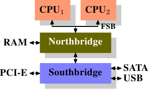
All CPUs (two in the previous example, but there can be more) are connected via a common bus (the Front Side Bus, FSB) to the Northbridge. The Northbridge contains, among other things, the memory controller, and its implementation determines the type of RAM chips used for the computer. Different types of RAM, such as DRAM, Rambus, and SDRAM, require different memory controllers.
To reach all other system devices, the Northbridge must communicate with the Southbridge. The Southbridge, often referred to as the I/O bridge, handles communication with devices through a variety of different buses. Today the PCI, PCI Express, SATA, and USB buses are of most importance, but PATA, IEEE 1394, serial, and parallel ports are also supported by the Southbridge. Older systems had AGP slots which were attached to the Northbridge. This was done for performance reasons related to insufficiently fast connections between the Northbridge and Southbridge. However, today the PCI-E slots are all connected to the Southbridge.
Such a system structure has a number of noteworthy consequences:
- All data communication from one CPU to another must travel over the same bus used to communicate with the Northbridge.
- All communication with RAM must pass through the Northbridge.
- The RAM has only a single port. {We will not discuss multi-port RAM in this document as this type of RAM is not found in commodity hardware, at least not in places where the programmer has access to it. It can be found in specialized hardware such as network routers which depend on utmost speed.}
- Communication between a CPU and a device attached to the Southbridge is routed through the Northbridge.
A couple of bottlenecks are immediately apparent in this design. One such bottleneck involves access to RAM for devices. In the earliest days of the PC, all communication with devices on either bridge had to pass through the CPU, negatively impacting overall system performance. To work around this problem some devices became capable of direct memory access (DMA). DMA allows devices, with the help of the Northbridge, to store and receive data in RAM directly without the intervention of the CPU (and its inherent performance cost). Today all high-performance devices attached to any of the buses can utilize DMA. While this greatly reduces the workload on the CPU, it also creates contention for the bandwidth of the Northbridge as DMA requests compete with RAM access from the CPUs. This problem, therefore, must to be taken into account.
A second bottleneck involves the bus from the Northbridge to the RAM. The exact details of the bus depend on the memory types deployed. On older systems there is only one bus to all the RAM chips, so parallel access is not possible. Recent RAM types require two separate buses (or channels as they are called for DDR2, see Figure 2.8) which doubles the available bandwidth. The Northbridge interleaves memory access across the channels. More recent memory technologies (FB-DRAM, for instance) add more channels.
With limited bandwidth available, it is important to schedule memory access in ways that minimize delays. As we will see, processors are much faster and must wait to access memory, despite the use of CPU caches. If multiple hyper-threads, cores, or processors access memory at the same time, the wait times for memory access are even longer. This is also true for DMA operations.
There is more to accessing memory than concurrency, however. Access patterns themselves also greatly influence the performance of the memory subsystem, especially with multiple memory channels. Refer to Section 2.2 for more details of RAM access patterns.
On some more expensive systems, the Northbridge does not actually contain the memory controller. Instead the Northbridge can be connected to a number of external memory controllers (in the following example, four of them).
Figure 2.2: Northbridge with External Controllers
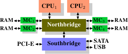
The advantage of this architecture is that more than one memory bus exists and therefore total bandwidth increases. This design also supports more memory. Concurrent memory access patterns reduce delays by simultaneously accessing different memory banks. This is especially true when multiple processors are directly connected to the Northbridge, as in Figure 2.2. For such a design, the primary limitation is the internal bandwidth of the Northbridge, which is phenomenal for this architecture (from Intel). {For completeness it should be mentioned that such a memory controller arrangement can be used for other purposes such as memory RAID which is useful in combination with hotplug memory.}
Using multiple external memory controllers is not the only way to increase memory bandwidth. One other increasingly popular way is to integrate memory controllers into the CPUs and attach memory to each CPU. This architecture is made popular by SMP systems based on AMD's Opteron processor. Figure 2.3 shows such a system. Intel will have support for the Common System Interface (CSI) starting with the Nehalem processors; this is basically the same approach: an integrated memory controller with the possibility of local memory for each processor.
Figure 2.3: Integrated Memory Controller
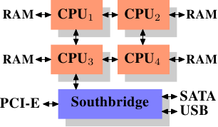
With an architecture like this there are as many memory banks available as there are processors. On a quad-CPU machine the memory bandwidth is quadrupled without the need for a complicated Northbridge with enormous bandwidth. Having a memory controller integrated into the CPU has some additional advantages; we will not dig deeper into this technology here.
There are disadvantages to this architecture, too. First of all, because the machine still has to make all the memory of the system accessible to all processors, the memory is not uniform anymore (hence the name NUMA - Non-Uniform Memory Architecture - for such an architecture). Local memory (memory attached to a processor) can be accessed with the usual speed. The situation is different when memory attached to another processor is accessed. In this case the interconnects between the processors have to be used. To access memory attached to CPU2 from CPU1 requires communication across one interconnect. When the same CPU accesses memory attached to CPU4 two interconnects have to be crossed.
Each such communication has an associated cost. We talk about NUMA factors when we describe the extra time needed to access remote memory. The example architecture in Figure 2.3 has two levels for each CPU: immediately adjacent CPUs and one CPU which is two interconnects away. With more complicated machines the number of levels can grow significantly. There are also machine architectures (for instance IBM's x445 and SGI's Altix series) where there is more than one type of connection. CPUs are organized into nodes; within a node the time to access the memory might be uniform or have only small NUMA factors. The connection between nodes can be very expensive, though, and the NUMA factor can be quite high.
Commodity NUMA machines exist today and will likely play an even greater role in the future. It is expected that, from late 2008 on, every SMP machine will use NUMA. The costs associated with NUMA make it important to recognize when a program is running on a NUMA machine. In Section 5 we will discuss more machine architectures and some technologies the Linux kernel provides for these programs.
Beyond the technical details described in the remainder of this section, there are several additional factors which influence the performance of RAM. They are not controllable by software, which is why they are not covered in this section. The interested reader can learn about some of these factors in Section 2.1. They are really only needed to get a more complete picture of RAM technology and possibly to make better decisions when purchasing computers.
The following two sections discuss hardware details at the gate level and the access protocol between the memory controller and the DRAM chips. Programmers will likely find this information enlightening since these details explain why RAM access works the way it does. It is optional knowledge, though, and the reader anxious to get to topics with more immediate relevance for everyday life can jump ahead to Section 2.2.5.
2.1 RAM Types
There have been many types of RAM over the years and each type varies, sometimes significantly, from the other. The older types are today really only interesting to the historians. We will not explore the details of those. Instead we will concentrate on modern RAM types; we will only scrape the surface, exploring some details which are visible to the kernel or application developer through their performance characteristics.
The first interesting details are centered around the question why there are different types of RAM in the same machine. More specifically, why there are both static RAM (SRAM {In other contexts SRAM might mean synchronous RAM.}) and dynamic RAM (DRAM). The former is much faster and provides the same functionality. Why is not all RAM in a machine SRAM? The answer is, as one might expect, cost. SRAM is much more expensive to produce and to use than DRAM. Both these cost factors are important, the second one increasing in importance more and more. To understand these difference we look at the implementation of a bit of storage for both SRAM and DRAM.
In the remainder of this section we will discuss some low-level details of the implementation of RAM. We will keep the level of detail as low as possible. To that end, we will discuss the signals at a logic level and not at a level a hardware designer would have to use. That level of detail is unnecessary for our purpose here.
2.1.1 Static RAM
Figure 2.4: 6-T Static RAM
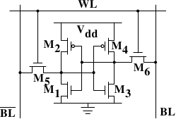
Figure 2.4 shows the structure of a 6 transistor SRAM cell. The core of this cell is formed by the four transistors M1 to M4 which form two cross-coupled inverters. They have two stable states, representing 0 and 1 respectively. The state is stable as long as power on Vdd is available.
If access to the state of the cell is needed the word access line WL is raised. This makes the state of the cell immediately available for reading on BL and BL. If the cell state must be overwritten the BL and BL lines are first set to the desired values and then WL is raised. Since the outside drivers are stronger than the four transistors (M1 through M4) this allows the old state to be overwritten.
See [sramwiki] for a more detailed description of the way the cell works. For the following discussion it is important to note that
- one cell requires six transistors. There are variants with four transistors but they have disadvantages.
- maintaining the state of the cell requires constant power.
- the cell state is available for reading almost immediately once the word access line WL is raised. The signal is as rectangular (changing quickly between the two binary states) as other transistor-controlled signals.
- the cell state is stable, no refresh cycles are needed.
There are other, slower and less power-hungry, SRAM forms available, but those are not of interest here since we are looking at fast RAM. These slow variants are mainly interesting because they can be more easily used in a system than dynamic RAM because of their simpler interface.
2.1.2 Dynamic RAM
Dynamic RAM is, in its structure, much simpler than static RAM. Figure 2.5 shows the structure of a usual DRAM cell design. All it consists of is one transistor and one capacitor. This huge difference in complexity of course means that it functions very differently than static RAM.
Figure 2.5: 1-T Dynamic RAM
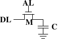
A dynamic RAM cell keeps its state in the capacitor C. The transistor M is used to guard the access to the state. To read the state of the cell the access line AL is raised; this either causes a current to flow on the data line DL or not, depending on the charge in the capacitor. To write to the cell the data line DL is appropriately set and then AL is raised for a time long enough to charge or drain the capacitor.
There are a number of complications with the design of dynamic RAM. The use of a capacitor means that reading the cell discharges the capacitor. The procedure cannot be repeated indefinitely, the capacitor must be recharged at some point. Even worse, to accommodate the huge number of cells (chips with 109 or more cells are now common) the capacity to the capacitor must be low (in the femto-farad range or lower). A fully charged capacitor holds a few 10's of thousands of electrons. Even though the resistance of the capacitor is high (a couple of tera-ohms) it only takes a short time for the capacity to dissipate. This problem is called leakage.
This leakage is why a DRAM cell must be constantly refreshed. For most DRAM chips these days this refresh must happen every 64ms. During the refresh cycle no access to the memory is possible. For some workloads this overhead might stall up to 50% of the memory accesses (see [highperfdram]).
A second problem resulting from the tiny charge is that the information read from the cell is not directly usable. The data line must be connected to a sense amplifier which can distinguish between a stored 0 or 1 over the whole range of charges which still have to count as 1.
A third problem is that charging and draining a capacitor is not instantaneous. The signals received by the sense amplifier are not rectangular, so a conservative estimate as to when the output of the cell is usable has to be used. The formulas for charging and discharging a capacitor are
![\[Formulas\]](https://static.lwn.net/images/cpumemory/capcharge.png)
This means it takes some time (determined by the capacity C and resistance R) for the capacitor to be charged and discharged. It also means that the current which can be detected by the sense amplifiers is not immediately available. Figure 2.6 shows the charge and discharge curves. The X—axis is measured in units of RC (resistance multiplied by capacitance) which is a unit of time.
Figure 2.6: Capacitor Charge and Discharge Timing
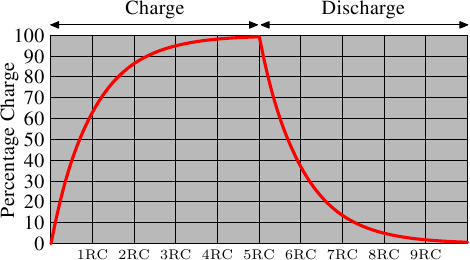
Unlike the static RAM case where the output is immediately available when the word access line is raised, it will always take a bit of time until the capacitor discharges sufficiently. This delay severely limits how fast DRAM can be.
The simple approach has its advantages, too. The main advantage is size. The chip real estate needed for one DRAM cell is many times smaller than that of an SRAM cell. The SRAM cells also need individual power for the transistors maintaining the state. The structure of the DRAM cell is also simpler and more regular which means packing many of them close together on a die is simpler.
Overall, the (quite dramatic) difference in cost wins. Except in specialized hardware — network routers, for example — we have to live with main memory which is based on DRAM. This has huge implications on the programmer which we will discuss in the remainder of this paper. But first we need to look into a few more details of the actual use of DRAM cells.
2.1.3 DRAM Access
A program selects a memory location using a virtual address. The processor translates this into a physical address and finally the memory controller selects the RAM chip corresponding to that address. To select the individual memory cell on the RAM chip, parts of the physical address are passed on in the form of a number of address lines.
It would be completely impractical to address memory locations individually from the memory controller: 4GB of RAM would require 232 address lines. Instead the address is passed encoded as a binary number using a smaller set of address lines. The address passed to the DRAM chip this way must be demultiplexed first. A demultiplexer with N address lines will have 2_N_ output lines. These output lines can be used to select the memory cell. Using this direct approach is no big problem for chips with small capacities.
But if the number of cells grows this approach is not suitable anymore. A chip with 1Gbit {I hate those SI prefixes. For me a giga-bit will always be 230 and not 109 bits.} capacity would need 30 address lines and 230 select lines. The size of a demultiplexer increases exponentially with the number of input lines when speed is not to be sacrificed. A demultiplexer for 30 address lines needs a whole lot of chip real estate in addition to the complexity (size and time) of the demultiplexer. Even more importantly, transmitting 30 impulses on the address lines synchronously is much harder than transmitting only 15 impulses. Fewer lines have to be laid out at exactly the same length or timed appropriately. {Modern DRAM types like DDR3 can automatically adjust the timing but there is a limit as to what can be tolerated.}
Figure 2.7: Dynamic RAM Schematic
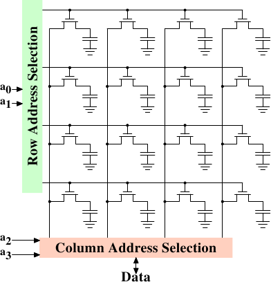
Figure 2.7 shows a DRAM chip at a very high level. The DRAM cells are organized in rows and columns. They could all be aligned in one row but then the DRAM chip would need a huge demultiplexer. With the array approach the design can get by with one demultiplexer and one multiplexer of half the size. {Multiplexers and demultiplexers are equivalent and the multiplexer here needs to work as a demultiplexer when writing. So we will drop the differentiation from now on.} This is a huge saving on all fronts. In the example the address lines a0 and a1 through the row address selection (RAS) demultiplexer select the address lines of a whole row of cells. When reading, the content of all cells is thusly made available to the column address selection (CAS) {The line over the name indicates that the signal is negated} multiplexer. Based on the address lines a2 and a3 the content of one column is then made available to the data pin of the DRAM chip. This happens many times in parallel on a number of DRAM chips to produce a total number of bits corresponding to the width of the data bus.
For writing, the new cell value is put on the data bus and, when the cell is selected using the RAS and CAS, it is stored in the cell. A pretty straightforward design. There are in reality — obviously — many more complications. There need to be specifications for how much delay there is after the signal before the data will be available on the data bus for reading. The capacitors do not unload instantaneously, as described in the previous section. The signal from the cells is so weak that it needs to be amplified. For writing it must be specified how long the data must be available on the bus after the RAS and CAS is done to successfully store the new value in the cell (again, capacitors do not fill or drain instantaneously). These timing constants are crucial for the performance of the DRAM chip. We will talk about this in the next section.
A secondary scalability problem is that having 30 address lines connected to every RAM chip is not feasible either. Pins of a chip are a precious resources. It is bad enough that the data must be transferred as much as possible in parallel (e.g., in 64 bit batches). The memory controller must be able to address each RAM module (collection of RAM chips). If parallel access to multiple RAM modules is required for performance reasons and each RAM module requires its own set of 30 or more address lines, then the memory controller needs to have, for 8 RAM modules, a whopping 240+ pins only for the address handling.
To counter these secondary scalability problems DRAM chips have, for a long time, multiplexed the address itself. That means the address is transferred in two parts. The first part consisting of address bits a0 and a1 in the example in Figure 2.7) select the row. This selection remains active until revoked. Then the second part, address bits a2 and a3, select the column. The crucial difference is that only two external address lines are needed. A few more lines are needed to indicate when the RAS and CAS signals are available but this is a small price to pay for cutting the number of address lines in half. This address multiplexing brings its own set of problems, though. We will discuss them in Section 2.2.
2.1.4 Conclusions
Do not worry if the details in this section are a bit overwhelming. The important things to take away from this section are:
- there are reasons why not all memory is SRAM
- memory cells need to be individually selected to be used
- the number of address lines is directly responsible for the cost of the memory controller, motherboards, DRAM module, and DRAM chip
- it takes a while before the results of the read or write operation are available
The following section will go into more details about the actual process of accessing DRAM memory. We are not going into more details of accessing SRAM, which is usually directly addressed. This happens for speed and because the SRAM memory is limited in size. SRAM is currently used in CPU caches and on-die where the connections are small and fully under control of the CPU designer. CPU caches are a topic which we discuss later but all we need to know is that SRAM cells have a certain maximum speed which depends on the effort spent on the SRAM. The speed can vary from only slightly slower than the CPU core to one or two orders of magnitude slower.
2.2 DRAM Access Technical Details
In the section introducing DRAM we saw that DRAM chips multiplex the addresses in order to save resources. We also saw that accessing DRAM cells takes time since the capacitors in those cells do not discharge instantaneously to produce a stable signal; we also saw that DRAM cells must be refreshed. Now it is time to put this all together and see how all these factors determine how the DRAM access has to happen.
We will concentrate on current technology; we will not discuss asynchronous DRAM and its variants as they are simply not relevant anymore. Readers interested in this topic are referred to [highperfdram] and [arstechtwo]. We will also not talk about Rambus DRAM (RDRAM) even though the technology is not obsolete. It is just not widely used for system memory. We will concentrate exclusively on Synchronous DRAM (SDRAM) and its successors Double Data Rate DRAM (DDR).
Synchronous DRAM, as the name suggests, works relative to a time source. The memory controller provides a clock, the frequency of which determines the speed of the Front Side Bus (FSB) — the memory controller interface used by the DRAM chips. As of this writing, frequencies of 800MHz, 1,066MHz, or even 1,333MHz are available with higher frequencies (1,600MHz) being announced for the next generation. This does not mean the frequency used on the bus is actually this high. Instead, today's buses are double- or quad-pumped, meaning that data is transported two or four times per cycle. Higher numbers sell so the manufacturers like to advertise a quad-pumped 200MHz bus as an effective 800MHz bus.
For SDRAM today each data transfer consists of 64 bits — 8 bytes. The transfer rate of the FSB is therefore 8 bytes multiplied by the effective bus frequency (6.4GB/s for the quad-pumped 200MHz bus). That sounds like a lot but it is the burst speed, the maximum speed which will never be surpassed. As we will see now the protocol for talking to the RAM modules has a lot of downtime when no data can be transmitted. It is exactly this downtime which we must understand and minimize to achieve the best performance.
2.2.1 Read Access Protocol
Figure 2.8: SDRAM Read Access Timing
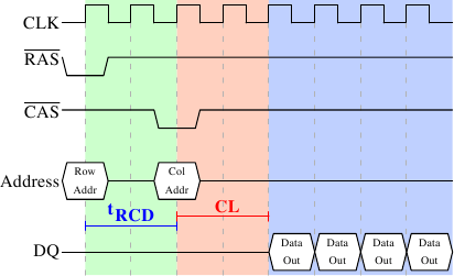
Figure 2.8 shows the activity on some of the connectors of a DRAM module which happens in three differently colored phases. As usual, time flows from left to right. A lot of details are left out. Here we only talk about the bus clock, RAS and CAS signals, and the address and data buses. A read cycle begins with the memory controller making the row address available on the address bus and lowering the RAS signal. All signals are read on the rising edge of the clock (CLK) so it does not matter if the signal is not completely square as long as it is stable at the time it is read. Setting the row address causes the RAM chip to start latching the addressed row.
The CAS signal can be sent after tRCD (RAS-to-CAS Delay) clock cycles. The column address is then transmitted by making it available on the address bus and lowering the CAS line. Here we can see how the two parts of the address (more or less halves, nothing else makes sense) can be transmitted over the same address bus.
Now the addressing is complete and the data can be transmitted. The RAM chip needs some time to prepare for this. The delay is usually called CAS Latency (CL). In Figure 2.8 the CAS latency is 2. It can be higher or lower, depending on the quality of the memory controller, motherboard, and DRAM module. The latency can also have half values. With CL=2.5 the first data would be available at the first falling flank in the blue area.
With all this preparation to get to the data it would be wasteful to only transfer one data word. This is why DRAM modules allow the memory controller to specify how much data is to be transmitted. Often the choice is between 2, 4, or 8 words. This allows filling entire lines in the caches without a new RAS/CAS sequence. It is also possible for the memory controller to send a new CAS signal without resetting the row selection. In this way, consecutive memory addresses can be read from or written to significantly faster because the RAS signal does not have to be sent and the row does not have to be deactivated (see below). Keeping the row open is something the memory controller has to decide. Speculatively leaving it open all the time has disadvantages with real-world applications (see [highperfdram]). Sending new CAS signals is only subject to the Command Rate of the RAM module (usually specified as T_x_, where x is a value like 1 or 2; it will be 1 for high-performance DRAM modules which accept new commands every cycle).
In this example the SDRAM spits out one word per cycle. This is what the first generation does. DDR is able to transmit two words per cycle. This cuts down on the transfer time but does not change the latency. In principle, DDR2 works the same although in practice it looks different. There is no need to go into the details here. It is sufficient to note that DDR2 can be made faster, cheaper, more reliable, and is more energy efficient (see [ddrtwo] for more information).
2.2.2 Precharge and Activation
Figure 2.8 does not cover the whole cycle. It only shows parts of the full cycle of accessing DRAM. Before a new RAS signal can be sent the currently latched row must be deactivated and the new row must be precharged. We can concentrate here on the case where this is done with an explicit command. There are improvements to the protocol which, in some situations, allows this extra step to be avoided. The delays introduced by precharging still affect the operation, though.
Figure 2.9: SDRAM Precharge and Activation
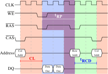
Figure 2.9 shows the activity starting from one CAS signal to the CAS signal for another row. The data requested with the first CAS signal is available as before, after CL cycles. In the example two words are requested which, on a simple SDRAM, takes two cycles to transmit. Alternatively, imagine four words on a DDR chip.
Even on DRAM modules with a command rate of one the precharge command cannot be issued right away. It is necessary to wait as long as it takes to transmit the data. In this case it takes two cycles. This happens to be the same as CL but that is just a coincidence. The precharge signal has no dedicated line; instead, some implementations issue it by lowering the Write Enable (WE) and RAS line simultaneously. This combination has no useful meaning by itself (see [micronddr] for encoding details).
Once the precharge command is issued it takes tRP (Row Precharge time) cycles until the row can be selected. In Figure 2.9 much of the time (indicated by the purplish color) overlaps with the memory transfer (light blue). This is good! But tRP is larger than the transfer time and so the next RAS signal is stalled for one cycle.
If we were to continue the timeline in the diagram we would find that the next data transfer happens 5 cycles after the previous one stops. This means the data bus is only in use two cycles out of seven. Multiply this with the FSB speed and the theoretical 6.4GB/s for a 800MHz bus become 1.8GB/s. That is bad and must be avoided. The techniques described in Section 6 help to raise this number. But the programmer usually has to do her share.
There is one more timing value for a SDRAM module which we have not discussed. In Figure 2.9 the precharge command was only limited by the data transfer time. Another constraint is that an SDRAM module needs time after a RAS signal before it can precharge another row (denoted as tRAS). This number is usually pretty high, in the order of two or three times the tRP value. This is a problem if, after a RAS signal, only one CAS signal follows and the data transfer is finished in a few cycles. Assume that in Figure 2.9 the initial CAS signal was preceded directly by a RAS signal and that tRAS is 8 cycles. Then the precharge command would have to be delayed by one additional cycle since the sum of tRCD, CL, and tRP (since it is larger than the data transfer time) is only 7 cycles.
DDR modules are often described using a special notation: w-x-y-z-T. For instance: 2-3-2-8-T1. This means:
| ----- |
| w | 2 | CAS Latency (CL) |
| x | 3 | RAS-to-CAS delay (tRCD) |
| y | 2 | RAS Precharge (tRP) |
| z | 8 | Active to Precharge delay (tRAS) |
| T | T1 | Command Rate |
There are numerous other timing constants which affect the way commands can be issued and are handled. Those five constants are in practice sufficient to determine the performance of the module, though.
It is sometimes useful to know this information for the computers in use to be able to interpret certain measurements. It is definitely useful to know these details when buying computers since they, along with the FSB and SDRAM module speed, are among the most important factors determining a computer's speed.
The very adventurous reader could also try to tweak a system. Sometimes the BIOS allows changing some or all these values. SDRAM modules have programmable registers where these values can be set. Usually the BIOS picks the best default value. If the quality of the RAM module is high it might be possible to reduce the one or the other latency without affecting the stability of the computer. Numerous overclocking websites all around the Internet provide ample of documentation for doing this. Do it at your own risk, though and do not say you have not been warned.
2.2.3 Recharging
A mostly-overlooked topic when it comes to DRAM access is recharging. As explained in Section 2.1.2, DRAM cells must constantly be refreshed. This does not happen completely transparently for the rest of the system. At times when a row {Rows are the granularity this happens with despite what [highperfdram] and other literature says (see [micronddr]).} is recharged no access is possible. The study in [highperfdram] found that [_s]urprisingly, DRAM refresh organization can affect performance dramatically_.
Each DRAM cell must be refreshed every 64ms according to the JEDEC specification. If a DRAM array has 8,192 rows this means the memory controller has to issue a refresh command on average every 7.8125µs (refresh commands can be queued so in practice the maximum interval between two requests can be higher). It is the memory controller's responsibility to schedule the refresh commands. The DRAM module keeps track of the address of the last refreshed row and automatically increases the address counter for each new request.
There is really not much the programmer can do about the refresh and the points in time when the commands are issued. But it is important to keep this part to the DRAM life cycle in mind when interpreting measurements. If a critical word has to be retrieved from a row which currently is being refreshed the processor could be stalled for quite a long time. How long each refresh takes depends on the DRAM module.
2.2.4 Memory Types
It is worth spending some time on the current and soon-to-be current memory types in use. We will start with SDR (Single Data Rate) SDRAMs since they are the basis of the DDR (Double Data Rate) SDRAMs. SDRs were pretty simple. The memory cells and the data transfer rate were identical.
Figure 2.10: SDR SDRAM Operation
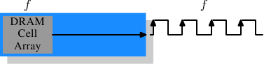
In Figure 2.10 the DRAM cell array can output the memory content at the same rate it can be transported over the memory bus. If the DRAM cell array can operate at 100MHz, the data transfer rate of the bus is thus 100Mb/s. The frequency f for all components is the same. Increasing the throughput of the DRAM chip is expensive since the energy consumption rises with the frequency. With a huge number of array cells this is prohibitively expensive. {Power = Dynamic Capacity × Voltage2 × Frequency.} In reality it is even more of a problem since increasing the frequency usually also requires increasing the voltage to maintain stability of the system. DDR SDRAM (called DDR1 retroactively) manages to improve the throughput without increasing any of the involved frequencies.
Figure 2.11: DDR1 SDRAM Operation
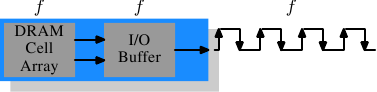
The difference between SDR and DDR1 is, as can be seen in Figure 2.11 and guessed from the name, that twice the amount of data is transported per cycle. I.e., the DDR1 chip transports data on the rising and falling edge. This is sometimes called a double-pumped bus. To make this possible without increasing the frequency of the cell array a buffer has to be introduced. This buffer holds two bits per data line. This in turn requires that, in the cell array in Figure 2.7, the data bus consists of two lines. Implementing this is trivial: one only has the use the same column address for two DRAM cells and access them in parallel. The changes to the cell array to implement this are also minimal.
The SDR DRAMs were known simply by their frequency (e.g., PC100 for 100MHz SDR). To make DDR1 DRAM sound better the marketers had to come up with a new scheme since the frequency did not change. They came with a name which contains the transfer rate in bytes a DDR module (they have 64-bit busses) can sustain:
100MHz × 64bit × 2 = 1,600MB/s
Hence a DDR module with 100MHz frequency is called PC1600. With 1600 > 100 all marketing requirements are fulfilled; it sounds much better although the improvement is really only a factor of two. {I will take the factor of two but I do not have to like the inflated numbers.}
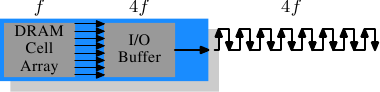
Figure 2.12: DDR2 SDRAM Operation
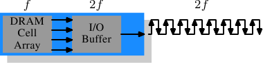
To get even more out of the memory technology DDR2 includes a bit more innovation. The most obvious change that can be seen in Figure 2.12 is the doubling of the frequency of the bus. Doubling the frequency means doubling the bandwidth. Since this doubling of the frequency is not economical for the cell array it is now required that the I/O buffer gets four bits in each clock cycle which it then can send on the bus. This means the changes to the DDR2 modules consist of making only the I/O buffer component of the DIMM capable of running at higher speeds. This is certainly possible and will not require measurably more energy, it is just one tiny component and not the whole module. The names the marketers came up with for DDR2 are similar to the DDR1 names only in the computation of the value the factor of two is replaced by four (we now have a quad-pumped bus). Figure 2.13 shows the names of the modules in use today.
| ----- |
| Array
Freq. | Bus
Freq. | Data
Rate | Name
(Rate) | Name
(FSB) |
| 133MHz | 266MHz | 4,256MB/s | PC2-4200 | DDR2-533 |
| 166MHz | 333MHz | 5,312MB/s | PC2-5300 | DDR2-667 |
| 200MHz | 400MHz | 6,400MB/s | PC2-6400 | DDR2-800 |
| 250MHz | 500MHz | 8,000MB/s | PC2-8000 | DDR2-1000 |
| 266MHz | 533MHz | 8,512MB/s | PC2-8500 | DDR2-1066 |
Figure 2.13: DDR2 Module Names
There is one more twist to the naming. The FSB speed used by CPU, motherboard, and DRAM module is specified by using the effective frequency. I.e., it factors in the transmission on both flanks of the clock cycle and thereby inflates the number. So, a 133MHz module with a 266MHz bus has an FSB frequency of 533MHz.
The specification for DDR3 (the real one, not the fake GDDR3 used in graphics cards) calls for more changes along the lines of the transition to DDR2. The voltage will be reduced from 1.8V for DDR2 to 1.5V for DDR3. Since the power consumption equation is calculated using the square of the voltage this alone brings a 30% improvement. Add to this a reduction in die size plus other electrical advances and DDR3 can manage, at the same frequency, to get by with half the power consumption. Alternatively, with higher frequencies, the same power envelope can be hit. Or with double the capacity the same heat emission can be achieved.
The cell array of DDR3 modules will run at a quarter of the speed of the external bus which requires an 8 bit I/O buffer, up from 4 bits for DDR2. See Figure 2.14 for the schematics.
Figure 2.14: DDR3 SDRAM Operation
Initially DDR3 modules will likely have slightly higher CAS latencies just because the DDR2 technology is more mature. This would cause DDR3 to be useful only at frequencies which are higher than those which can be achieved with DDR2, and, even then, mostly when bandwidth is more important than latency. There is already talk about 1.3V modules which can achieve the same CAS latency as DDR2. In any case, the possibility of achieving higher speeds because of faster buses will outweigh the increased latency.
One possible problem with DDR3 is that, for 1,600Mb/s transfer rate or higher, the number of modules per channel may be reduced to just one. In earlier versions this requirement held for all frequencies, so one can hope that the requirement will at some point be lifted for all frequencies. Otherwise the capacity of systems will be severely limited.
Figure 2.15 shows the names of the expected DDR3 modules. JEDEC agreed so far on the first four types. Given that Intel's 45nm processors have an FSB speed of 1,600Mb/s, the 1,866Mb/s is needed for the overclocking market. We will likely see more of this towards the end of the DDR3 lifecycle.
| ----- |
| Array
Freq. | Bus
Freq. | Data
Rate | Name
(Rate) | Name
(FSB) |
| 100MHz | 400MHz | 6,400MB/s | PC3-6400 | DDR3-800 |
| 133MHz | 533MHz | 8,512MB/s | PC3-8500 | DDR3-1066 |
| 166MHz | 667MHz | 10,667MB/s | PC3-10667 | DDR3-1333 |
| 200MHz | 800MHz | 12,800MB/s | PC3-12800 | DDR3-1600 |
| 233MHz | 933MHz | 14,933MB/s | PC3-14900 | DDR3-1866 |
Figure 2.15: DDR3 Module Names
All DDR memory has one problem: the increased bus frequency makes it hard to create parallel data busses. A DDR2 module has 240 pins. All connections to data and address pins must be routed so that they have approximately the same length. Even more of a problem is that, if more than one DDR module is to be daisy-chained on the same bus, the signals get more and more distorted for each additional module. The DDR2 specification allow only two modules per bus (aka channel), the DDR3 specification only one module for high frequencies. With 240 pins per channel a single Northbridge cannot reasonably drive more than two channels. The alternative is to have external memory controllers (as in Figure 2.2) but this is expensive.
What this means is that commodity motherboards are restricted to hold at most four DDR2 or DDR3 modules. This restriction severely limits the amount of memory a system can have. Even old 32-bit IA-32 processors can handle 64GB of RAM and memory demand even for home use is growing, so something has to be done.
One answer is to add memory controllers into each processor as explained in Section 2. AMD does it with the Opteron line and Intel will do it with their CSI technology. This will help as long as the reasonable amount of memory a processor is able to use can be connected to a single processor. In some situations this is not the case and this setup will introduce a NUMA architecture and its negative effects. For some situations another solution is needed.
Intel's answer to this problem for big server machines, at least for the next years, is called Fully Buffered DRAM (FB-DRAM). The FB-DRAM modules use the same components as today's DDR2 modules which makes them relatively cheap to produce. The difference is in the connection with the memory controller. Instead of a parallel data bus FB-DRAM utilizes a serial bus (Rambus DRAM had this back when, too, and SATA is the successor of PATA, as is PCI Express for PCI/AGP). The serial bus can be driven at a much higher frequency, reverting the negative impact of the serialization and even increasing the bandwidth. The main effects of using a serial bus are
- more modules per channel can be used.
- more channels per Northbridge/memory controller can be used.
- the serial bus is designed to be fully-duplex (two lines).
An FB-DRAM module has only 69 pins, compared with the 240 for DDR2. Daisy chaining FB-DRAM modules is much easier since the electrical effects of the bus can be handled much better. The FB-DRAM specification allows up to 8 DRAM modules per channel.
Compared with the connectivity requirements of a dual-channel Northbridge it is now possible to drive 6 channels of FB-DRAM with fewer pins: 2×240 pins versus 6×69 pins. The routing for each channel is much simpler which could also help reducing the cost of the motherboards.
Fully duplex parallel busses are prohibitively expensive for the traditional DRAM modules, duplicating all those lines is too costly. With serial lines (even if they are differential, as FB-DRAM requires) this is not the case and so the serial bus is designed to be fully duplexed, which means, in some situations, that the bandwidth is theoretically doubled alone by this. But it is not the only place where parallelism is used for bandwidth increase. Since an FB-DRAM controller can run up to six channels at the same time the bandwidth can be increased even for systems with smaller amounts of RAM by using FB-DRAM. Where a DDR2 system with four modules has two channels, the same capacity can handled via four channels using an ordinary FB-DRAM controller. The actual bandwidth of the serial bus depends on the type of DDR2 (or DDR3) chips used on the FB-DRAM module.
We can summarize the advantages like this:
| ----- |
| | DDR2 | FB-DRAM |
|
| | | | Pins | 240 | 69 |
| Channels | 2 | 6 |
| DIMMs/Channel | 2 | 8 |
| Max Memory | 16GB | 192GB |
| Throughput | ~10GB/s | ~40GB/s |
There are a few drawbacks to FB-DRAMs if multiple DIMMs on one channel are used. The signal is delayed—albeit minimally—at each DIMM in the chain, which means the latency increases. But for the same amount of memory with the same frequency FB-DRAM can always be faster than DDR2 and DDR3 since only one DIMM per channel is needed; for large memory systems DDR simply has no answer using commodity components.
2.2.5 Conclusions
This section should have shown that accessing DRAM is not an arbitrarily fast process. At least not fast compared with the speed the processor is running and with which it can access registers and cache. It is important to keep in mind the differences between CPU and memory frequencies. An Intel Core 2 processor running at 2.933GHz and a 1.066GHz FSB have a clock ratio of 11:1 (note: the 1.066GHz bus is quad-pumped). Each stall of one cycle on the memory bus means a stall of 11 cycles for the processor. For most machines the actual DRAMs used are slower, thusly increasing the delay. Keep these numbers in mind when we are talking about stalls in the upcoming sections.
The timing charts for the read command have shown that DRAM modules are capable of high sustained data rates. Entire DRAM rows could be transported without a single stall. The data bus could be kept occupied 100%. For DDR modules this means two 64-bit words transferred each cycle. With DDR2-800 modules and two channels this means a rate of 12.8GB/s.
But, unless designed this way, DRAM access is not always sequential. Non-continuous memory regions are used which means precharging and new RAS signals are needed. This is when things slow down and when the DRAM modules need help. The sooner the precharging can happen and the RAS signal sent the smaller the penalty when the row is actually used.
Hardware and software prefetching (see Section 6.3) can be used to create more overlap in the timing and reduce the stall. Prefetching also helps shift memory operations in time so that there is less contention at later times, right before the data is actually needed. This is a frequent problem when the data produced in one round has to be stored and the data required for the next round has to be read. By shifting the read in time, the write and read operations do not have to be issued at basically the same time.
2.3 Other Main Memory Users
Beside the CPUs there are other system components which can access the main memory. High-performance cards such as network and mass-storage controllers cannot afford to pipe all the data they need or provide through the CPU. Instead, they read or write the data directly from/to the main memory (Direct Memory Access, DMA). In Figure 2.1 we can see that the cards can talk through the South- and Northbridge directly with the memory. Other buses, like USB, also require FSB bandwidth—even though they do not use DMA—since the Southbridge is connected to the Northbridge through the FSB, too.
While DMA is certainly beneficial, it means that there is more competition for the FSB bandwidth. In times with high DMA traffic the CPU might stall more than usual while waiting for data from the main memory. There are ways around this given the right hardware. With an architecture as in Figure 2.3 one can make sure the computation uses memory on nodes which are not affected by DMA. It is also possible to attach a Southbridge to each node, equally distributing the load on the FSB of all the nodes. There are a myriad of possibilities. In Section 6 we will introduce techniques and programming interfaces which help achieving the improvements which are possible in software.
Finally it should be mentioned that some cheap systems have graphics systems without separate, dedicated video RAM. Those systems use parts of the main memory as video RAM. Since access to the video RAM is frequent (for a 1024x768 display with 16 bpp at 60Hz we are talking 94MB/s) and system memory, unlike RAM on graphics cards, does not have two ports this can substantially influence the systems performance and especially the latency. It is best to ignore such systems when performance is a priority. They are more trouble than they are worth. People buying those machines know they will not get the best performance.
Continue to:
- Part 2 (CPU caches)
- Part 3 (Virtual memory)
- Part 4 (NUMA systems)
- Part 5 (What programmers can do - cache optimization)
- Part 6 (What programmers can do - multi-threaded optimizations)
- Part 7 (Memory performance tools)
- Part 8 (Future technologies)
- Part 9 (Appendices and bibliography)
(Log in to post comments)
Nice
Posted Sep 21, 2007 20:34 UTC (Fri) by tcoppi (guest, #44423) [Link]
Very well written and informative. Looking forward to rest!
This is great!
Posted Sep 21, 2007 21:39 UTC (Fri) by socket (guest, #43) [Link]
I've been looking for exactly this document for a long time now! Thanks, Ulrich, and LWN!
This is great!
Posted Sep 21, 2007 22:04 UTC (Fri) by ikm (subscriber, #493) [Link]
Same here :) Great work!
This is great!
Posted Sep 21, 2007 22:42 UTC (Fri) by nix (subscriber, #2304) [Link]
Ulrich's documentation is basically always amazing. I'll admit to having a
google alert on his homepage specifically so that I can read everything he
writes as he releases it.
This is great!
Posted Oct 11, 2007 4:04 UTC (Thu) by vaib (guest, #48292) [Link]
Can you please tell the homepage of the author.
This is great!
Posted Oct 11, 2007 21:55 UTC (Thu) by nix (subscriber, #2304) [Link]
Warning: Ulrich has no patience at all with people who don't do their
homework (by, say, typing in `ulrich drepper home page' in Google).
It's <http://people.redhat.com/drepper/>.
What every programmer should know about memory, Part 1
Posted Sep 21, 2007 21:48 UTC (Fri) by Coren (guest, #39136) [Link]
Thanks a lot. This first part is really of a great quality.
64 processors?
Posted Sep 21, 2007 22:03 UTC (Fri) by roelofs (guest, #2599) [Link]
...will be a computer with up to four sockets, each filled with a quad core CPU that, in the case of Intel CPUs, will be hyper-threaded. This means the standard system in the data center will have up to 64 virtual processors.
Is there a 4-way hyperthreading variant I haven't heard about? I thought HT was always viewed as two CPUs by the Linux kernel (well, assuming it's enabled in the BIOS and the kernel config), which would imply no more than 32 virtual processors. Did I miss something here?
Greg
64 processors?
Posted Sep 21, 2007 22:41 UTC (Fri) by ms (subscriber, #41272) [Link]
I'm not totally sure what the author's referring to, but hyper threading is coming back. Of course, the Sun Niagara chip does 4 threads per core, rather than two, and IBM's Power series has been doing SMT (hyper threading by another name) for some time. http://anandtech.com/cpuchipsets/intel/showdoc.aspx?i=310... talks about 8 core Intel CPUs that will support hyper threading per core for 16 threads per CPU.
64 processors?
Posted Sep 22, 2007 21:57 UTC (Sat) by deater (subscriber, #11746) [Link]
Please realize that Intel's "Hyperthreading" is not the same as "Multi-threading" as implemented by other vendors. Hyperthreading will often give you worse performance than simply using one core (ie, turning hyperthreading off).
Multi-threading, as in real SMT, will actually give you a performance improvement, but just not a linear one like adding an extra full core would. For example, extra hardware threads on the Niagara give about the same improvement as about 50% of a CPU.
I've done tests to verify this on our servers, and as a result I disable Hyperthreading on all of our compute nodes. Don't take my word for it though, run tests yourself.
64 processors?
Posted Sep 23, 2007 15:33 UTC (Sun) by alankila (guest, #47141) [Link]
In my experience, running almost any two perl tasks in parallel on a HT tends to take longer in wallclock time than running the two one after the other (keeping the other hyperthread idle). The difference is not large, but it tends to be a few percentage points slower with hyperthreading than without.
I pondered this for a while, and thought that it might be because each hyperthread in turn pushes the cached data of the other hyperthread off the cpu, resulting in expensive memory re-fetches which in this case actually negate the advantage of utilizing the idle CPU computation units.
Even so, I'd still keep HT enabled for web servers and like. This is because the small loss in throughput is likely to be repaid by a small decrease of system latency. Two processors, even two "half-speed" ones, can still do two tasks at the same time, and short computation bursts can well occur faster thanks to increased likelihood of there being an idle core immediately available for the task.
64 processors?
Posted Sep 24, 2007 15:47 UTC (Mon) by giraffedata (subscriber, #1954) [Link]
thought that it might be because each hyperthread in turn pushes the cached data of the other hyperthread off the cpu, resulting in expensive memory re-fetches which in this case actually negate the advantage of utilizing the idle CPU computation units.
It's roughly that effect, but this actual scenario doesn't happen, because a hyperthread timeslice lasts only until the next cache miss and there is more than one line of cache. The point of hyperthreading is to let Thread B run while Thread A is waiting to get stuff into cache.
However, you do have the simple problem of having only half the locality in the memory cache. If two threads are in greatly different contexts, each will get half the cache and half a cache might make it take significantly longer to get something done than a whole cache.
But I think the usual reason for hyperthreading slowdown is just the overhead of switching threads. If that exceeds the time you would sit idle waiting for memory access in the single thread case, the double thread has less throughput than the single thread.
What should have been said along with the 50% number above is that it is just for some highly average workload. The effect of hyperthreading has a great deal to do with how much memory access the programs do. A system that spends most of its time moving stuff around in memory will not benefit from hyperthreading. But a system that spends half its time accessing memory and the other half computing in registers and near caches might get close to double the throughput with 2 hyperthreads.
I usually turn off hyperthreading just to restore consistency. Otherwise, my speed varies almost randomly.
64 processors?
Posted Sep 25, 2007 10:05 UTC (Tue) by alankila (guest, #47141) [Link]
Thanks for a highly informative clarification.
Hyperthreading performance
Posted Oct 4, 2007 20:10 UTC (Thu) by anton (subscriber, #25547) [Link]
But I think the usual reason for hyperthreading slowdown is just the overhead of switching threads.
In SMT (and that includes hyperthreading), there is no thread switching overhead. The execution core just executes instructions from different contexts at the same time (but in different resources).
I don't know why the Pentium 4 variant of SMT performs as badly as it does; cache thrashing may contribute, but I don't think that this is the main reason. The main reasons are probably some obscure microarchitectural details, maybe the replay system, maybe something else.
64 processors?
Posted Sep 26, 2007 10:16 UTC (Wed) by epa (subscriber, #39769) [Link]
I don't think that is a fair comparison. You would need to compare running two perl tasks in parallel with HT versus running two in parallel without HT. That will tell you whether HT itself gives any performance improvement for parallel-perl workloads, and so may give a clue about whether to enable it on a production web server (which presumably is running lots of perl jobs at once).
Whether your two programs are best scheduled in parallel or serially is another question - as you found out, it may be faster to run one then the other. This does not necessarily imply that hyperthreading should be turned off.
64 processors?
Posted Sep 25, 2007 19:09 UTC (Tue) by csnook (guest, #36935) [Link]
Hyperthreading is generally not a win on workloads that are already well-optimized. If the application is making effective use of the cache, and is compiled to minimize pipeline bubbles, hyperthreading will just reduce your cache hit rate.
The problem that Hyperthreading solves quite well is workloads that cannot be well-optimized because they react to unpredictable external events, as is the case with web servers. It's also beneficial on desktop systems where having only one CPU can harm interactivity while background tasks are running, but in the age of multicore CPUs that won't be much of an issue.
As a rule of thumb, the more performance tuning you're doing on a system, the more likely it is you'll want to disable Hyperthreading. HPC nodes and centralized database servers definitely suffer, while build systems and static web servers definitely benefit.
What every programmer should know about memory, Part 1
Posted Sep 21, 2007 23:00 UTC (Fri) by jwb (guest, #15467) [Link]
Very nice article. You did address power issues obliquely when talking about DDR3, but I'm surprised you didn't mention the power drawbacks of FB-DIMM. The fast shift register on each DIMM requires a few watts more than a standard DDR2 module. And when you add more DIMMs to an FB-DIMM system, all memory access becomes slower, not just access to DIMMs at the end of chains. For example on a particular system I have here memory performance is best with 4 FB-DIMMs and a bit slower with 8.
What every programmer should know about memory, Part 1
Posted Sep 23, 2007 8:23 UTC (Sun) by TRS-80 (subscriber, #1804) [Link]
AMD's next server socket will put four buffers per socket on the motherboard and otherwise use regular DDR3 DIMMs. Which is kind of like the external memory controller scenario, but connected direct to the CPU. Intel is rumoured to be developing something similar called AMB2.
What every programmer should know about memory, Part 1
Posted Sep 25, 2007 14:10 UTC (Tue) by wretcheddawn (guest, #47780) [Link]
Where do you find these 69 pin fb-dimms. It looks like everything I can find on newegg is 240 pin fb-dimms?
FB-DIMM pins
Posted Oct 4, 2007 20:16 UTC (Thu) by anton (subscriber, #25547) [Link]
Actually only the interface at the memory controller is 69 pins (allowing more channels from one memory controller chip). The FB-DIMM needs these 69 pins, plus 69 pins to talk to the next FB-DIMM, plus additional pins for power and ground; that's why they have the familiar 240-pin form factor.
banks?
Posted Sep 22, 2007 4:33 UTC (Sat) by sbishop (guest, #33061) [Link]
For such a detailed and well-written article, I'm surprised that banks weren't mentioned. In short, a memory chip contains 4 or 8 banks, which each contain rows, which each contain columns. With regards to the timing constraints mentioned regarding rows, each bank is almost completely independent. Behaviourly, this means that you can activate, read, write and precharge each bank concurrently. (There's only one shared data bus, of course, but this allows you to talk to one bank while another is busy internally.)
I work for a memory manufacturer, but I don't know much about how our stuff is actually used. So maybe this doesn't actually help, speed-wise, and that's why Ulrich didn't mention it.
I have a few other comments/suggestions:
- I wouldn't bother mentioning half-latencies. DDR only had one, 2.5, but DDR2 and beyond don't have any.
- Speaking of CAS latencies, they're only getting worse. Higher clock speeds means higher latencies, period. You could run DDR parts at CAS latency 2, 2.5, or 3. DDR2 latencies go from 3 up to 7, I believe.
- I don't understand the foot-note part of this quote: "As explained in Section 2.1.2, DRAM cells must constantly be refreshed. This does not happen completely transparently for the rest of the system. At times when a row {Rows are the granularity this happens with despite what [highperfdram] and other literature says (see [micronddr]).} is recharged no access is possible."
I don't know what the literature says--Can we get links to that stuff?--but all banks have to be precharged during a refresh event. (To be specific, this is an "auto-refresh"--"self-refresh" is a low-power mode.)
Sam Bishop
No banks, thnx.
Posted Sep 22, 2007 10:21 UTC (Sat) by khim (subscriber, #9252) [Link]
While there are subtle differences between two-banks DIMM and two single-bank DIMMs (related to refresh as you've correctly pointed out) from software point of view they are more-or-less identical. I think this is why it was omitted from article. And the question "what the hell does latency 2.5 mean?" is common (less so today when DDR is almost history and DDR2 is mainstream, but still) so I think few lines are worth it...
No banks, thnx.
Posted Sep 22, 2007 14:10 UTC (Sat) by sbishop (guest, #33061) [Link]
You're confusing the terms "banks" and "ranks."
Ulrich goes into quite a bit of detail about how an address is broken into a "row" and "column" component, but there is a third component, bank, internal to the DRAM.
A DIMM1 can be single-rank or dual-rank. When you write or read a single-rank DIMM, you talk to every memory component on the DIMM, every time. Dual-rank DIMMs have double the number of components as a single-rank DIMM, and when you write or read (activate or precharge, for that matter) you only talk to half of the components.
What any of this has to do with software, I don't know. I work with some absolutely lousy programmers who know quite a bit more about memory than I do. :)
1 I know this holds for unbuffered DIMMs, but I don't know about fully-buffered DIMMs. I don't work with those.
CAS
Posted Sep 22, 2007 14:39 UTC (Sat) by knan (subscriber, #3940) [Link]
And currently available DDR3 modules looks to have CAS latencies of 5 to 9.
banks?
Posted Sep 24, 2007 13:52 UTC (Mon) by vapier (subscriber, #15768) [Link]
unfortunately, the memory management in Linux is completely transparent to userspace which means the advantages of placing your data in different banks is totally not doable.
it's really only possible when you're writing your own bare-metal applications as then you have full control over the physical memory layout. your custom linker scripts would place the data such that you make sure specific pieces of data lie in specific banks.
of course, this is beyond the stated scope as it isnt Linux :)
banks?
Posted Sep 24, 2007 16:54 UTC (Mon) by sbishop (guest, #33061) [Link]
Now you've got the Gentoo crowd double checking their linker man page... :)
Seriously, I've heard that the translation from a physical address to a particular bank/row/column combination is specific to the memory controller. Which makes perfect sense.
Also, let me make this clear: my bank comment was in regards to the "more details than you really need to know" section anyway. With Linux and/or random, commodity hardware, you can't call out a specific row or column either. But if you're going to talk about rows and columns, you ought to at least mention banks, the third address component of a modern DRAM. ("Modern DRAM" here means, approximately, anything I'm familiar with: Sync-DRAM, DDR, DDR2, etc.)
banks?
Posted Sep 24, 2007 20:18 UTC (Mon) by vapier (subscriber, #15768) [Link]
i might point out that linker scripts arent documented in the linker man page
i obviously cant read minds, but i think the discussion of being able to scan rows without re-issuing a CAS command will lead into the idea of accessing data in a certain fashion (in sequential lines) rather than much more randomly ... whereas with banks, exhibiting certain behavior at runtime wont matter since in general, being in different banks is random
What every programmer should know about memory, Part 1
Posted Sep 22, 2007 17:20 UTC (Sat) by ttonino (guest, #4073) [Link]
DRAM data has to be written back after every read: there is just enough charge in a cell to give a readable output on the bit line. That data must be written back when changing to another line.
What every programmer should know about memory, Part 1
Posted Sep 22, 2007 17:42 UTC (Sat) by dskoll (subscriber, #1630) [Link]
DRAM data has to be written back after every read
That happens automatically. The sense amplifiers form a positive feedback loop that restores the charge in the capacitor. In fact, a refresh is performed just by doing a read (but throwing away the data.)
on-board video cards
Posted Sep 22, 2007 22:32 UTC (Sat) by ccyoung (guest, #16340) [Link]
almost every rack-mount server I use has onboard video (I use Tyan and Super Micro).
since it's only used when building the system, does it matter?
how do you know if the RAM is it's own or shared?
on-board video cards
Posted Sep 23, 2007 11:48 UTC (Sun) by khim (subscriber, #9252) [Link]
It does not matter if GPU is only used while system is initially set up: it will still suck performance from system. That said most server motherboards nowadays have old, slow, yet dedicated GPU with separate memory chip - exactly to free system bus...
You can use lspci and Google to find out what kind of GPU chip is used and if it's using dedicated RAM or system RAM...
on-board video cards
Posted Sep 24, 2007 16:06 UTC (Mon) by giraffedata (subscriber, #1954) [Link]
I assume the performance sucking comes from the fact that the video controller is constantly reading from the memory to refresh the screen, even if no one is looking at it or no monitor is plugged in.
Modern computers have power-saving features that disable the display after a period of no keyboard/mouse activity. Does that shut down the refresh in the video controller, thus eliminating the performance impact?
What about DVI? VGA CRTs have to be refreshed constantly, from the video controller (and a VGA LCD monitor, emulating a CRT, would too), but what about DVI LCD display?
on-board video cards
Posted Sep 24, 2007 19:34 UTC (Mon) by khim (subscriber, #9252) [Link]
DVI requires constant refresh too. It's not needed for modern LCD - that's just how DVI is designed.
As for needless polling when monitor is power save mode... Few years ago it was certainly true anyway - but times are changing. May be latest integrated CPUs are stopping this useless polling when there are no need, I just don't know.
on-board video cards
Posted Sep 28, 2007 14:41 UTC (Fri) by pm101 (guest, #3011) [Link]
Are you sure?
My impression was that active matrix LCDs worked a lot like DRAM. They had a transistor and a capacitor for each pixel (the transistor was added in the move from passive to active matrix), but the voltage on that capacitor decayed and needed to be periodically refreshed. I was unaware of LCD displays having any on-board memory from which to do the refresh, but that could have been added while I wasn't following the market, although I'd be surprised, since it seems like it'd be an unnecessary cost item.
on-board video cards
Posted Sep 29, 2007 21:49 UTC (Sat) by giraffedata (subscriber, #1954) [Link]
It's not the physics, but the modernness that I think makes the refresh not necessary for LCDs at the level it is for CRTs: If I were designing a monitor in the 1990s out of parts that need to be refreshed (even a CRT), I would put required refresh function inside,rather than pass the responsibility off to the computer. In SVGA days, though, it probably made sense to keep the monitor dumb.
But I guess DVI designers decided the computer wants to update the picture by a full raster scan 60 times a second anyway, so there's no need for internal refresh. Doing a little reading just now, it looks like the DVI data stream is a simple raster scan. It even apparently has "blanking intervals," though they couldn't possibly be for same purpose as on a CRT.
on-board video cards
Posted Sep 29, 2007 23:06 UTC (Sat) by foom (subscriber, #14868) [Link]
But I guess DVI designers decided the computer wants to update the picture by a full raster scan 60 times a second anyway, so there's no need for internal refresh. Doing a little reading just now, it looks like the DVI data stream is a simple raster scan. It even apparently has "blanking intervals," though they couldn't possibly be for same purpose as on a CRT.
DVI's timing and blanking intervals are the same as VGA's. I believe it was designed this way to make the modification to the video cards easier, and to facilitate dual-output DVI / VGA video cards. (so the VGA port is basically just the DVI port with an extra D2A converter in the path.)
reply from super micro
Posted Sep 24, 2007 19:12 UTC (Mon) by ccyoung (guest, #16340) [Link]
"The onboard PCI intergraded VGA card (ATIES 1000) has its own 16MB
memory, and it will not share with the memory from DIMMs."
what I expected / hoped, but did not find in their doc.
my guess the same for other better server motherboards - after this article am seeing why they're an extra $100.
on-board video cards
Posted Sep 24, 2007 10:30 UTC (Mon) by etienne_lorrain@yahoo.fr (guest, #38022) [Link]
since it's only used when building the system, does it matter?
And also if the server uses a text mode display, it should not load
more than 80402 contigous bytes sixty times per second - shared
memory should not be a problem - isn't it?
What every programmer should know about memory, Part 1
Posted Sep 23, 2007 9:50 UTC (Sun) by sylware (guest, #35259) [Link]
Perfect balance.
What every programmer should know about memory, Part 1
Posted Sep 23, 2007 15:19 UTC (Sun) by Trou.fr (subscriber, #26289) [Link]
Excellent article, thank you :)
What every programmer should know about memory, Part 1
Posted Sep 23, 2007 17:13 UTC (Sun) by rkklinux (subscriber, #42417) [Link]
Excellent! Looks I can't wait for subsequents publications. Requesting editor for single PS or PDF file that includes all seven segments.
PDF version
Posted Sep 23, 2007 19:04 UTC (Sun) by corbet (editor, #1) [Link]
My understanding is that Ulrich plans to make the full PDF available once the full series has been published.
What every programmer should know about memory, Part 1
Posted Sep 23, 2007 19:16 UTC (Sun) by asamardzic (guest, #27161) [Link]
Requesting editor for single PS or PDF file that includes all seven segments.
This series is announced by U. Drepper some time ago, see here (mhm, and few day ago I grumbled here at linking to blogs...); it is mentioned there that PDF will be released once this series completed.
As all commenters above, I enjoyed reading first installment. However, I think also there are segments that could be further improved, in order to really have this text as ultimate reference for memory related topics. For example, static RAM diagram could be explained better (remember that this text is directed towards programmers, that may have not much EE related background), as well as DRAM refreshing (it is left somewhat unclear how DRAM cell is returned to its initial value after practically destroying this value during read operation - this is say much more clear at block diagram from corresponding Wikipedia article than from Figure 2.7 from text above), etc. That sort of stuff is usually explained in all of its glory detail in digital logic design books (for example in [Katz/Boririello][90] seminal work), but maybe it could be worth trying to digest it for this kind of text too...
Repetition
Posted Sep 23, 2007 21:36 UTC (Sun) by intgr (subscriber, #39733) Link][91
Here's a little grammar fix for the article:
It is limited to commodity hardware and and further limited to a subset of that hardware.
Note that these technical details tend to change rapidly, so the the reader is advised to take the date of this writing into account.
Repetition
Posted Sep 24, 2007 12:24 UTC (Mon) by malor (guest, #2973) Link][92
Another little fix:
"reverting negative impact of the serialization and even increase the bandwidth."
would be more grammatically correct as,
"reverting the negative impact of the serialization and even increasing the bandwidth."
(add "the", add "ing".)
You could also drop "the" before both serialization and bandwidth, for improved flow. If it were my sentence, I'd write it this way:
"... reverting the negative impact of serialization, and even increasing total bandwidth."
Another grammar fix
Posted Sep 27, 2007 21:41 UTC (Thu) by rmunn (guest, #40618) Link][93
I spotted another grammar oops. In section 2 ("Commodity Hardware Today"), seventh paragraph (the one immediately after the first bullet-point list), the last sentence reads: "This problem, therefore, must to be taken into account." That should be either "needs to be taken into account" or "must be taken into account."
This is, of course, an artifact of editing the paper, where "needs to be" was changed into "must be" at some point but the leftover "to" was missed.
Wonderful article, many thanks to Ulrich and our editor
Posted Sep 23, 2007 22:44 UTC (Sun) by pr1268 (subscriber, #24648) Link][94
Outstanding article! I look forward to reading § 3-7 when they're released. Thank you, Ulrich, for considering LWN as a medium on which to publish your paper, and thanks to our editor for honoring Ulrich's request. This (and many other fine articles) make me feel that my subscription to LWN is money well spent.
Bibliography sure would be nice
Posted Sep 24, 2007 1:01 UTC (Mon) by foom (subscriber, #14868) Link][95
Hate to complain, but seeing [interestingsoundingreferences], and not being able to
see what they're actually referencing is somewhat irritating. I'd be fine with a separate page just
containing the biblio for the whole paper if the holdup is that it's too hard to linkify the refs in each
section.
What every programmer should know about memory, Part 1
Posted Sep 24, 2007 13:21 UTC (Mon) by tyhik (guest, #14747) Link][96
Ulrich has written fantastic technical papers earlier. Immediately, before reading, I was sure this one is not going to be different. Great thanks Ulrich! Can't wait for subsequent installments. Thanks also to lwn.
I think it's an error here. Section 2.3: "... since the Southbridge is connected to the Northbridge through the FSB, too."
AFAIK the bridges are not connected to each other through FSB.
Bridges connected to each other through FSB
Posted Sep 24, 2007 16:17 UTC (Mon) by giraffedata (subscriber, #1954) Link][97
AFAIK the bridges are not connected to each other through FSB.
And at the top of the article, it basically says that (and shows it in a drawing).
A similar contention question left open is that of contention in the Northbridge. Can that be a bottleneck? And what is it for, anyway? One could imagine the memory controller being directly on the FSB.
Bridges connected to each other through FSB
Posted Sep 26, 2007 18:20 UTC (Wed) by csnook (guest, #36935) Link][98
The northbridge is the barrier between the CPU domain (FSB, HT, etc.), which has to deal with cache coherency, locking, interrupt delivery, etc. and the rest of the system, which simply passes serial messages or parallel data/address tuples around. On a sufficiently primitive system you don't really need one, but all modern commodity microarchitectures have something like a northbridge either on the chipset or the processor itself.
As for bottlenecks, even if the northbridge itself has enough internal bandwidth between all of its ports to function in a non-blocking fashion, you can't have a bottleneck-free network unless both the CPU and the I/O controllers have dedicated bandwidth to the memory. That only makes sense with multi-port DRAM, which isn't used for main memory in any commodity system.
What every programmer should know about memory, Part 1
Posted Sep 26, 2007 20:18 UTC (Wed) by dankamongmen (subscriber, #35141) Link][99
Ulrich's amazing, and the main source of my understandings of modern glibc / linux-userspace API. Thanks again for such execellent code and attending documentation!
What every programmer should know about memory, Part 1
Posted Sep 26, 2007 21:22 UTC (Wed) by k8to (subscriber, #15413) Link][100
I cannot help but be a sourpuss and say: almost no programmer neeeds to know this about memory.
Some architects on software that needs good optimization should probably be acquiainted with the performance characteristics discussed, but the none of them need be aware of the circuit design. None.
What every programmer should know about memory, Part 1
Posted Sep 27, 2007 8:09 UTC (Thu) by tyhik (guest, #14747) Link][101
"... but the none of them need be aware of the circuit design. None."
There are programmers out there, who write memory controller configuration code for boot loaders. I have done it and knowing the electrical design of memory cells really helped to answer simple questions like why the hell does DRAM need a configurable controller while the onchip SRAM is nicely ready for use right after powerup.
What every programmer should know about memory, Part 1
Posted Sep 28, 2007 15:56 UTC (Fri) by pm101 (guest, #3011) Link][102
Personally, I think it is useful to have a reasonable knowledge one level of abstraction down, and one level of abstraction up. There are a number of reasons for this:
- You can often find optimizations that cross abstraction barriers. It is difficult to predict what you'll need to know to do this, so you really need to have a deep understanding of both layers. In some cases, you can also influence the hardware design.
- You can predict how the technology may evolve.
- You gain intellectual depth. This is especially important for systems programmers -- the target of this article. If I'm designing a kernel, or a virtual machine (as in JVM, or .net runtime), or a high-performance systems library, I want to design it in such a way that it can take advantage of possible future underlying technologies.
Indeed, in many cases, I may even be able to influence underlying technologies. If I am aware of the circuit requirements of memory refresh, I can design code that explicitly leaves time for the refresh, while giving good bandwidth and latency when the memory is actually accessed. If something is a good idea, and a major OS or runtime can take advantage of it, you can bet that hardware designers somewhere will add support for it.
The major reason most CPUs only have 2-4 cores today, and didn't have multiple cores a while ago, was that software could not take advantage of them. Right now, optimum performance comes from about 64 cores at 700MHz each (the Tilera processor), but it can only be used in esoteric applications because software designers a decade ago were not aware of where the hardware is headed, and did not design applications, languages, or run-times in a parallelism-friendly way (programmer-friendly parallelism is only starting to happen today with languages like Fortress).
What every programmer should know about memory, Part 1
Posted Sep 30, 2007 20:27 UTC (Sun) by k8to (subscriber, #15413) Link][103
Agreed. But knowing how a dram cell is implemented is more than one level of abstraction below low-level programming, and that is more than one level of abstraction below what "every" programmer will ever deal with.
Reader Comments
Posted Sep 26, 2007 23:25 UTC (Wed) by drepper (subscriber, #5153) Link][104
I appreciate (most of) the comments and actually made already a few changes based on them to clarify a few things (and correct typos etc).
But I'm not going to reply to anything specific here and now. This is just section 2 (with 1 only being an introduction). Some of what has been discussed in comments goes far beyond what is in these sections. Once you've read section 6 you probably have a better understanding about what is covered and what isn't (and to some extend: why certain things are covered in the first place).
So, don't regard my silence as a sign of disinterest, it just means that many questions will automatically be answered later.
Reader Comments
Posted Oct 1, 2007 22:22 UTC (Mon) by roelofs (guest, #2599) Link][105
Two more clarification-comments:
Recent RAM types require two separate buses (or channels as they are called for DDR2, see Figure 2.8) which doubles the available bandwidth.
Unless I'm missing something fundamental, Figure 2.8 has nothing to do with DDR2 channels. Indeed, I don't believe the comment even refers to Figures 2.12 or 2.13; I see nothing relevant. Perhaps the figure in question was dropped at some point?
In this example the SDRAM spits out one word per cycle.
Here and in several other places, the text is ambiguous. "Cycle" in this context apparently means clock cycle, but there's an implicit (larger) cycle measured from RAS to RAS (for example) that defines the overall throughput. Figure 2.8 actually shows four words going out in that larger cycle.
Greg
Hooray!
Posted Sep 27, 2007 14:42 UTC (Thu) by dwheeler (guest, #1216) Link][106
I'm delighted to see this series, thanks for running it. It's always frustrated me that people who develop software often have no clue what's going on underneath, and as a result write hideous code. E.G., yes, it does matter what order you access matrices in. I presume this series will eventually get there.
Also: let me say that I like the SI binary prefixes (GiByte, etc.); when computer memories were 48K, the difference between the binary and decimal prefixes didn't matter much, but as everything is getting bigger/faster, the differences have getting bigger too. When you're being imprecise, it doesn't matter, but when you want to be precise (e.g., when describing product specs or presenting a diagnostic report), I find them REALLY helpful. In some circumstances it's also the law: claiming your product does something, but not actually meeting your claims (because you used the wrong prefix) can actually get you hauled into court. There's a much bigger world beyond computing, and they already know what "Giga" means; it's 10^9.
Hooray!
Posted Nov 11, 2007 6:24 UTC (Sun) by zooko (guest, #2589) Link][107
When we dealt with numbers in the thousands (10^3), approximating a kilo as 2^10 was only 2.5%
off.  Now that we routinely deal with numbers in the billions (10^9), approximating a giga as
2^30 is 7.5% off.  Some of us already deal with numbers in the trillions (10^12), and
approximating a tera as 2^40 is a full 10% off!

Now if you do binary arithmetic in your head, so that when you see 14,463,188,475,466, you
instantly know that it is 13.2 * 2^40, then this comment doesn't apply to you.  But you don't.
When you see "14,463,188,475,466" you approximate it in your head as "14.5 gigs".  If you tell
someone else that you are looking at 14.5 gigs, and they think that you mean 14.5 2^40's, then
they are overestimating the number you are looking at by more than 10%!

See also:

<http://en.wikipedia.org/wiki/SI_prefix>

A "kilo" has meant 10^3 to the scientific world since 1795.  A "tera" has meant 10^12 since
1960.  Programmers use of units are eventually going to have to become compatible with the
larger scientific world, not least because the numbers we deal with are getting bigger.
Hooray!
Posted Nov 11, 2007 6:28 UTC (Sun) by zooko (guest, #2589) Link][108
Argh -- I shouldn't post to LWN while sleepy.

While lecturing people about the value of using precise terminology, I accidentally wrote
"gigs" when I meant "teras".

If it had been gigs, the people in the example would have been only 7.5% off.

Sorry about that.
What every programmer should know about memory, Part 1
Posted Sep 27, 2007 19:36 UTC (Thu) by jvestby (guest, #3087) Link][109
Excellent stuff.
I believe I have found a small typo in the formula just above figure 2.12.
Something like 133MHz is needed to get 1600.
What every programmer should know about memory, Part 1
Posted Sep 27, 2007 20:06 UTC (Thu) by Unleashed (guest, #47573) Link][110
Hey, this article and the likes you can find here just made me finally decide to subscribe! Bravo Ulrich!
Good article (so far)
Posted Sep 28, 2007 19:51 UTC (Fri) by filker0 (guest, #31278) Link][111
The article here is primarily about x86 type systems, assumes (I think) 64 bit multi-core CPUs, and also assumes a general computing environment. Extending this to other architectures might make it more useful (not that it's not a good overview so far; I learned a few things, and it's only 1/7th of the way through) to the folks this will matter the most to -- the embedded Linux programmer. Embedded programmers have more control over their environment than typical user-space programmers, and often need to tweak things to get rid of every wasted cycle possible.
Better knowing how the memory works, how it's connected to the rest of the system, and how software can be written to take this into account can lead to better performance. If this is applied at the kernel level when organizing kernel data structures and code, as well as in the design of service code (DMA, paging, interrupt handlers, data streams/pipes, IPC, etc.) could lead to better system performance.
Thanks for the article. I look forward to the rest of the parts.
Grammar correction
Posted Oct 1, 2007 3:47 UTC (Mon) by valankar (subscriber, #5992) Link][112
"Implementing this is trivial: one only has the use the same column address for two DRAM cells and access them in parallel."
should be:
"Implementing this is trivial: one only has to use the same column address for two DRAM cells and access them in parallel."
What every programmer should know about memory, Part 1
Posted Oct 3, 2007 14:19 UTC (Wed) by wyrdwright (guest, #4747) Link][113
Excellent article; clear and concise without sacrificing too much detail. Looking forward to the rest.
100MHz × 64bit × 2 = 1,600MB/s ?
Posted Oct 4, 2007 6:15 UTC (Thu) by pdfan (guest, #48029) Link][114
100MHz × 64bit × 2 = 1,600MB/s
bash-3.2# bc
bc 1.06
Copyright 1991-1994, 1997, 1998, 2000 Free Software Foundation, Inc.
This is free software with ABSOLUTELY NO WARRANTY.
For details type `warranty'.
100 * 64 * 2
12800
100 * 64 * 2 / 8
1600
quit
bash-3.2#
100MHz × 64bit × 2 = 1,600MB/s ?
Posted Dec 4, 2007 4:52 UTC (Tue) by sgifford (guest, #49399) Link][115
I was confused by the same thing; throughout section 2.2.4 it wasn't clear to me whether MB/s
meant megabytes/second or megabits/second.  Usually this abbreviation means megabytes, but the
text implied that it was megabits.  Clearing this up would make that section much... err...
clearer.

Even with that, a great article!  Thanks!
What every programmer should know about memory, Part 1
Posted Oct 4, 2007 16:44 UTC (Thu) by tjrtech (guest, #48047) Link][116
Great article and good review. I learned all this as a formally educated computer engineer. This shows why computer engineers write faster code than comp sci or informally trained coders.
What every programmer should know about memory, Part 1
Posted Oct 5, 2007 11:18 UTC (Fri) by jschrod (subscriber, #1646) Link][117
Well, it depends where you study. At the TU Darmstadt, Germany, this stuff was part of our undergrad Computer Science courses, back in 1981ff. (I don't know the current curricula, though.)
What every programmer should know about memory, Part 1
Posted Oct 5, 2007 15:33 UTC (Fri) by edmcman (guest, #48105) Link][118
A wonderful and professional article!
As a side note, does anyone know what this was written in, and perhaps what the diagrams were created in?
The tools used
Posted Oct 5, 2007 15:51 UTC (Fri) by corbet (editor, #1) Link][119
All done in LaTeX and metapost. Conversion to HTML was done by a script I wrote after I gave up on all the more general LaTeX->HTML tools out there.
The tools used
Posted Nov 19, 2007 7:46 UTC (Mon) by Ford_Prefect (subscriber, #36934) Link][120
Is the script publishable? Might save a lot of people a lot of trouble.
What every programmer should know about memory, Part 1
Posted Oct 5, 2007 19:43 UTC (Fri) by njs (guest, #40338) Link][121
For the diagrams, see:
http://udrepper.livejournal.com/12663.html
http://udrepper.livejournal.com/12840.html
What every programmer should know about memory, Part 1
Posted Oct 10, 2007 15:34 UTC (Wed) by DonDiego (guest, #24141) Link][122
An Intel Core 2 processor running at 2.933GHz and a 1.066GHz FSB have a clock ratio of 11:1 (note: the 1.066GHz bus is quad-pumped). Each stall of one cycle on the memory bus means a stall of 11 cycles for the processor.
11:1? I thought it was ~3:1, what have I missed there? It does not look like a typo...
What every programmer should know about memory, Part 1
Posted Oct 10, 2007 22:22 UTC (Wed) by wookey (subscriber, #5501) Link][123
You have missed the bit that the '1.066Ghz' bus is 'quad-pumped' so isn't really 1GHz at all: it is a quarter of that. Hence about 11:1 rather than about 3:1 ration between clock speeds. I just learned this from the above article (I had been taken in by marketers before and assumed that FSB speeds were real :-)
What every programmer should know about memory, Part 1
Posted Jan 6, 2014 10:26 UTC (Mon) by RohitS5 (guest, #94785) Link][124
This are the kind of details which makes difference between a good programmer and an average programmer. I am surprised to see how much more to learn in this space with time, memory, threading, processing etc. [Thank you][125]
Still very useful and informative
Posted Apr 3, 2015 7:17 UTC (Fri) by zenk (guest, #99503) Link][126
I am surprised that almost 8 years passed, this article is still very useful and informative.
Nowadays performance is almost always related to memory performance, the information and rationale is more useful.
Thank you Ulrich and LWN!
What every programmer should know about memory, Part 1
Posted Nov 18, 2017 11:23 UTC (Sat) by cncwebworld (guest, #119731) Link][127
Very good compiled article
Copyright © 2007, Eklektix, Inc.
Comments and public postings are copyrighted by their creators.
Linux is a registered trademark of Linus Torvalds
[90]: [91]: https://lwn.net/Articles/251110/ [92]: https://lwn.net/Articles/251137/ [93]: https://lwn.net/Articles/251961/ [94]: https://lwn.net/Articles/251111/ [95]: https://lwn.net/Articles/251114/ [96]: https://lwn.net/Articles/251146/ [97]: https://lwn.net/Articles/251189/ [98]: https://lwn.net/Articles/251639/ [99]: https://lwn.net/Articles/251735/ [100]: https://lwn.net/Articles/251750/ [101]: https://lwn.net/Articles/251811/ [102]: https://lwn.net/Articles/252058/ [103]: https://lwn.net/Articles/252389/ [104]: https://lwn.net/Articles/251767/ [105]: https://lwn.net/Articles/252586/ [106]: https://lwn.net/Articles/251879/ [107]: https://lwn.net/Articles/258053/ [108]: https://lwn.net/Articles/258054/ [109]: https://lwn.net/Articles/251940/ [110]: https://lwn.net/Articles/251948/ [111]: https://lwn.net/Articles/252091/ [112]: https://lwn.net/Articles/252415/ [113]: https://lwn.net/Articles/252817/ [114]: https://lwn.net/Articles/253026/ [115]: https://lwn.net/Articles/260837/ [116]: https://lwn.net/Articles/253152/ [117]: https://lwn.net/Articles/253317/ [118]: https://lwn.net/Articles/253360/ [119]: https://lwn.net/Articles/253368/ [120]: https://lwn.net/Articles/259080/ [121]: https://lwn.net/Articles/253417/ [122]: https://lwn.net/Articles/253854/ [123]: https://lwn.net/Articles/253899/ [124]: https://lwn.net/Articles/579273/ [125]: http://javarevisited.blogspot.com [126]: https://lwn.net/Articles/638981/ [127]: https://lwn.net/Articles/739519/